-
- PCB TYPE
- PRINTED CIRCUIT BOARD PROTOTYPE ALUMINUM PRINTED CIRCUIT BOARD R&F PCB FPC HIGH FREQUENCY PCB HIGH-TG PCB HEAVY COPPER PCB HDI PCB PCB FOR LIGHTING METAL CORE PCB
time:Nov 18. 2025, 13:52:22
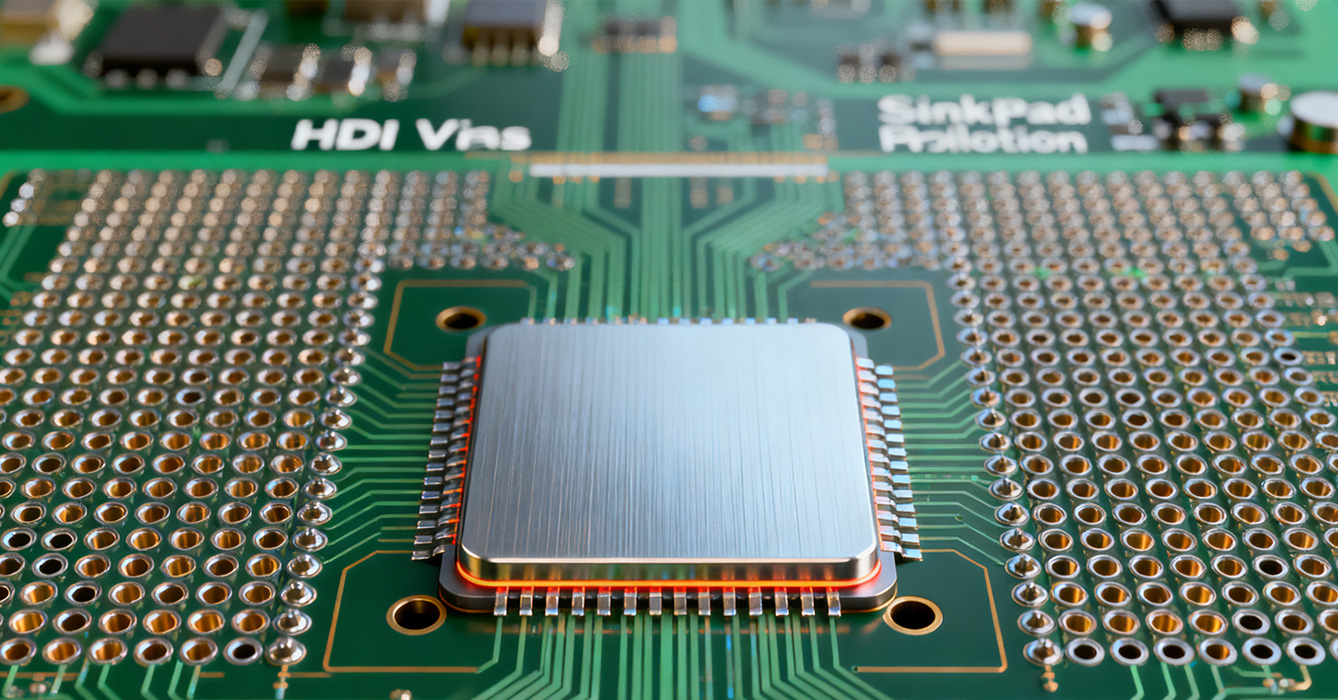
As electronic devices evolve toward extreme miniaturization and higher power densities, the demand for PCB solutions that balance high-density interconnects (HDI) and efficient thermal management has become critical. The HDI Vias Sinkpad PCB Solution addresses this dual challenge by merging HDI’s microvia technology with the thermal efficiency of sinkpad structures, creating a unified system that eliminates trade-offs between connectivity density and heat dissipation. This innovative approach is transformative for industries ranging from premium consumer electronics to industrial IoT, where compact form factors and reliable high-power operation are non-negotiable. By integrating microvias directly within sinkpad designs, engineers can achieve tighter component spacing, shorter signal paths, and enhanced thermal transfer—all while maintaining structural integrity and signal integrity. This article explores the core value proposition, design synergies, application landscapes, manufacturing advancements, and future directions of the HDI Vias Sinkpad PCB Solution.
The effectiveness of this solution stems from the seamless integration of HDI via technology and sinkpad thermal design, leveraging the strengths of each to overcome traditional limitations.
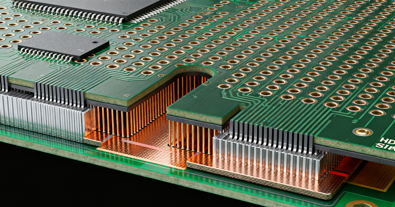
HDI vias—including blind, buried, and microvias—enable vertical connectivity between PCB layers without consuming valuable surface area, while sinkpads provide dedicated thermal pathways for high-power components. The key synergy lies in aligning microvia arrays within sinkpad regions to create vertical thermal channels, accelerating heat transfer from component junctions to internal ground planes or cooling structures. Unlike conventional designs where vias and heat sinks compete for space, this solution uses copper-filled microvias to enhance both electrical connectivity and thermal conductivity, as the conductive fill material eliminates air gaps that impede heat flow. This integration reduces thermal resistance while maximizing routing density, a critical advantage for devices with stacked components or fine-pitch packages.
Traditional PCB designs often require separate areas for thermal management and interconnects, leading to larger board footprints. The HDI Vias Sinkpad Solution eliminates this inefficiency by co-locating microvias within sinkpad boundaries. Microvias placed directly under component pads (via-in-pad technology) enable fan-out routing without extending beyond the sinkpad’s thermal area, preserving the sinkpad’s heat-spreading capability while supporting high I/O count components. This co-location strategy reduces PCB size by up to 30% compared to discrete HDI and sinkpad implementations, making it ideal for ultra-compact devices like wearables and miniaturized industrial sensors.
The combination of HDI vias and sinkpads improves long-term reliability by addressing two common failure points: thermal cycling-induced delamination and signal degradation. Sinkpads distribute heat evenly across the PCB, minimizing temperature gradients that cause material fatigue, while HDI’s microvia structures—with their smaller aspect ratios and robust fill materials—resist cracking from thermal expansion mismatches. Additionally, shorter signal paths enabled by HDI vias reduce impedance mismatches and signal delays, ensuring stable electrical performance even as components operate at elevated temperatures. This reliability is critical for mission-critical applications such as medical devices and aerospace electronics.

The HDI Vias Sinkpad PCB Solution excels in applications where high-density packaging and thermal efficiency are equally critical, enabling innovation across key industries.
Smartphones, AR/VR headsets, and portable gaming devices benefit from this solution’s ability to accommodate high-performance chips (e.g., multi-core processors and high-resolution display drivers) in ultra-thin form factors. Microvia arrays within sinkpads support dense component routing while dissipating heat from power-hungry components, preventing thermal throttling and ensuring smooth user experiences. The space-saving design also enables sleeker product silhouettes without compromising functionality.
Industrial sensors, edge AI modules, and compact controllers operate in harsh environments with limited cooling options. The HDI Vias Sinkpad Solution’s robust thermal management protects components from extreme temperature fluctuations, while its high-density interconnects support the integration of multiple sensors and communication modules on a single board. This reduces system complexity and improves reliability in factory automation, smart grid, and remote monitoring applications.
Medical devices such as portable diagnostic tools and implantable monitors require both miniaturization and absolute reliability. The solution’s low-profile design and efficient heat dissipation meet strict size constraints, while HDI’s precise interconnects ensure accurate signal transmission for sensitive sensors. In aerospace, the solution’s weight-saving benefits and resistance to vibration-induced damage make it suitable for satellite communication modules and UAV navigation systems.

Successful implementation of the HDI Vias Sinkpad Solution requires careful design coordination to balance thermal, electrical, and mechanical requirements.
Designers must align microvia placement with sinkpad geometry to avoid disrupting thermal pathways. Microvias should be distributed evenly across the sinkpad area to maintain uniform heat transfer, while avoiding clustering that could create hotspots. Using filled and plated-over vias prevents solder wicking during assembly, preserving both the sinkpad’s thermal contact and the via’s electrical integrity. Additionally, via-in-pad configurations must be optimized to maintain solder joint strength, ensuring mechanical stability for surface-mount components.
HDI’s build-up layer structure offers flexibility to integrate dedicated thermal planes adjacent to sinkpad regions. Layer stackups should be designed to maximize heat transfer from sinkpads to internal thermal planes via microvias, while maintaining controlled impedance for high-speed signals. Separating analog and digital ground planes—connected through strategic via placement—minimizes electromagnetic interference (EMI), a critical consideration for dense interconnect environments. This layered approach ensures thermal efficiency does not compromise signal quality.
The choice of materials must support both HDI processing and thermal performance. Low-dielectric-constant substrates enhance signal integrity for high-speed interconnects, while high-thermal-conductivity core materials (e.g., copper-clad laminates with enhanced thermal properties) boost the sinkpad’s heat-dissipating capability. Compatibility between substrate materials and via fill materials is essential to prevent delamination, especially under thermal cycling. Advanced materials like graphene-enhanced laminates are emerging as options to further improve thermal conductivity without sacrificing HDI processability.

Producing HDI Vias Sinkpad PCBs requires precision manufacturing techniques to achieve both high-density interconnects and consistent thermal performance.
Laser drilling technology is critical for creating the small apertures required for HDI vias, ensuring accuracy and minimal thermal impact on surrounding materials. Ultra-short pulse lasers enable drilling of microvias with smooth walls, improving plating adhesion and thermal conductivity. For copper-filled vias, pulse plating or horizontal jet plating processes ensure uniform fill and consistent electrical/thermal performance across the board. These techniques address the challenge of maintaining via integrity while working within the constraints of sinkpad thickness and material properties.
Achieving reliable integration of HDI layers and sinkpad structures requires tight control during lamination. Vacuum lamination processes eliminate air gaps between layers, enhancing thermal transfer and structural stability. Precision alignment systems—with tolerances measured in micrometers—ensure microvias align perfectly with sinkpad regions and internal thermal planes. This alignment is critical to avoid disconnects in thermal or electrical pathways, which would compromise the solution’s performance.
Quality control must validate both interconnect integrity and thermal efficiency. Automated optical inspection (AOI) and X-ray testing verify via fill quality and layer alignment, while thermal imaging and resistance testing confirm the sinkpad’s heat-dissipating capability. These dual-quality checks ensure the solution meets both electrical and thermal specifications, reducing the risk of field failures in critical applications.

The HDI Vias Sinkpad PCB Solution is poised for further advancement as electronic systems push the boundaries of density and power.
As ultra-HDI technology advances, microvia sizes continue to shrink, enabling even higher interconnect densities. Future solutions may incorporate sub-2-mil microvias paired with ultra-thin sinkpad structures, supporting next-generation chip-scale packages with unprecedented I/O density. This miniaturization will extend the solution’s applicability to micro-electronics and wearable devices.
Emerging trends include embedding temperature sensors within sinkpad regions, enabling real-time thermal monitoring. Paired with HDI’s high-speed interconnects, these smart sinkpads can trigger dynamic cooling adjustments, optimizing performance and extending component lifespan. This integration of sensing and thermal management will be critical for AI-driven devices with variable power demands.
The industry’s shift toward sustainability is driving innovations in eco-friendly materials and processes for HDI Vias Sinkpad PCBs. Water-soluble substrates and recyclable thermal materials are being explored, while process optimizations reduce energy consumption and waste. These advancements align the solution with global environmental goals without compromising performance.
The HDI Vias Sinkpad PCB Solution represents a pivotal advancement in addressing the conflicting demands of miniaturization, high-density interconnects, and thermal management in modern electronics. By integrating HDI’s microvia technology with the thermal efficiency of sinkpads, this solution eliminates traditional trade-offs, enabling smaller, more powerful, and reliable devices across consumer, industrial, medical, and aerospace sectors. Successful implementation requires careful design coordination, precision manufacturing, and material synergy—all supported by ongoing technological advancements. As electronic systems continue to evolve, the HDI Vias Sinkpad PCB Solution will remain a cornerstone technology, empowering engineers to push the boundaries of what is possible in high-performance, compact electronic design. For manufacturers and designers, adopting this integrated approach is key to staying competitive in an era where density and efficiency define success.

Got project ready to assembly? Contact us: info@apollopcb.com


We're not around but we still want to hear from you! Leave us a note:

Leave Message to APOLLOPCB
