-
- PCB TYPE
- PRINTED CIRCUIT BOARD PROTOTYPE ALUMINUM PRINTED CIRCUIT BOARD R&F PCB FPC HIGH FREQUENCY PCB HIGH-TG PCB HEAVY COPPER PCB HDI PCB PCB FOR LIGHTING METAL CORE PCB
time:Nov 18. 2025, 13:55:14
RF Application Sinkpad Vias PCB has become a cornerstone technology for high-frequency electronic systems, addressing the dual challenges of signal integrity (SI) preservation and thermal management in radio frequency (RF) applications. Unlike standard PCBs, this specialized design integrates sinkpad structures—dedicated metal cores for heat dissipation—with optimized via configurations tailored to mitigate parasitic effects at frequencies ranging from hundreds of MHz to tens of GHz. As RF systems evolve toward higher power densities, smaller form factors, and extreme operating environments (from satellite communication to radar systems), sinkpad vias PCBs enable the reliable performance critical for industries such as aerospace, telecommunications, and defense. This article explores the core design synergies, material considerations, application-specific optimizations, and industry best practices that define effective RF Application Sinkpad Vias PCB solutions.
The success of RF Application Sinkpad Vias PCB lies in harmonizing thermal dissipation with the strict signal requirements of high-frequency systems, where even minor design flaws can cause significant performance degradation.
RF vias inherently introduce parasitic inductance and capacitance, which disrupt impedance matching and cause signal reflection at high frequencies. Sinkpad integration addresses this by leveraging the metal core as a stable reference plane, minimizing impedance discontinuities. Designers optimize via geometry—prioritizing smaller diameters and reduced pad sizes—to limit parasitic capacitance, while integrating the sinkpad as a continuous ground reference to provide low-impedance return paths for RF signals. Additionally, eliminating via stubs through blind/buried via technology or back drilling prevents resonant effects that would otherwise degrade signal quality, ensuring seamless signal transmission across layers without compromising thermal conductivity.
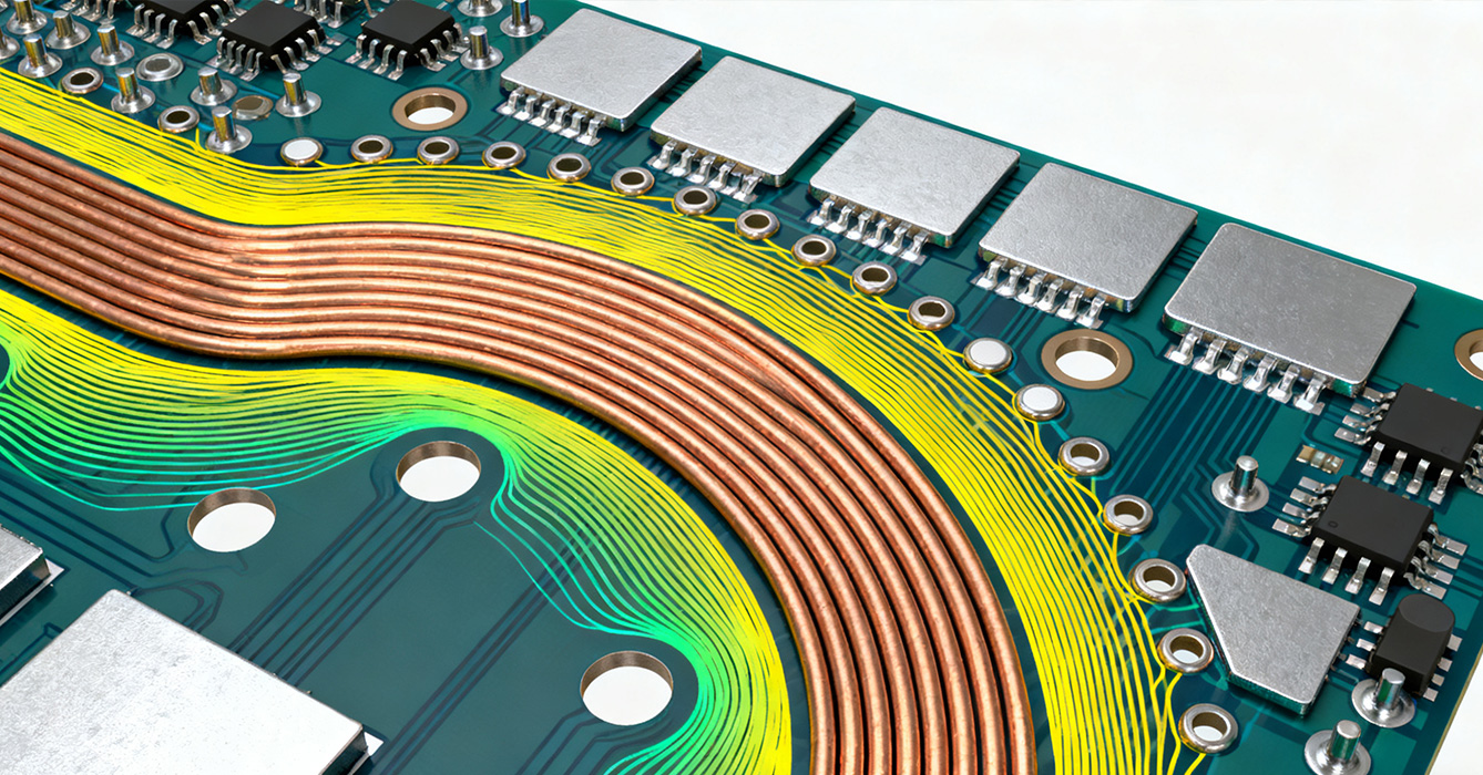
Sinkpad vias are strategically placed to facilitate heat transfer from high-power RF components (such as power amplifiers and transceivers) while avoiding interference with critical signal paths. The metal sinkpad core acts as a thermal conduit, channeling heat away from active components through vias to inner layers or external cooling systems. By separating thermal vias from signal vias—with adequate spacing to prevent crosstalk—designers maintain both efficient heat dissipation and signal integrity. This coexistence is critical in dense RF systems, where overheating can exacerbate signal distortion and reduce component lifespan.
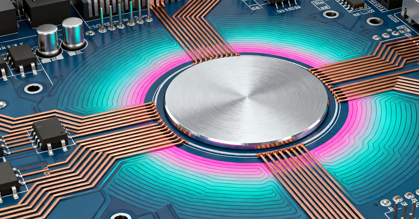
The sinkpad’s metal core serves as an enhanced ground plane for RF circuits, reducing electromagnetic interference (EMI) and improving shielding. Surrounding signal vias with arrays of ground vias creates a low-inductance shield, confining RF energy and minimizing radiation loss. This ground via placement—aligned with the sinkpad’s continuous ground structure—suppresses crosstalk between adjacent RF paths and external noise, a key requirement for sensitive applications like satellite communication and radar. The sinkpad’s integrity is preserved by avoiding ground plane splits near vias, ensuring uninterrupted current return paths and stable impedance characteristics.

Material selection for RF Application Sinkpad Vias PCB is driven by the need to balance thermal conductivity, dielectric stability, and low signal loss—critical factors for high-frequency operation.
RF systems demand substrates with stable dielectric constants and minimal loss tangent to reduce signal attenuation. High-performance materials such as PTFE-based laminates, Rogers composites, and modified polyimide (PI) are preferred over standard FR4, as they maintain electrical stability across wide frequency ranges and temperature fluctuations. These substrates are paired with sinkpad cores of aluminum or copper for optimal thermal transfer, creating a hybrid structure that supports both RF performance and heat dissipation. For extreme environments (e.g., space or industrial settings), radiation-resistant substrate coatings and corrosion-protective finishes enhance durability without degrading dielectric properties.
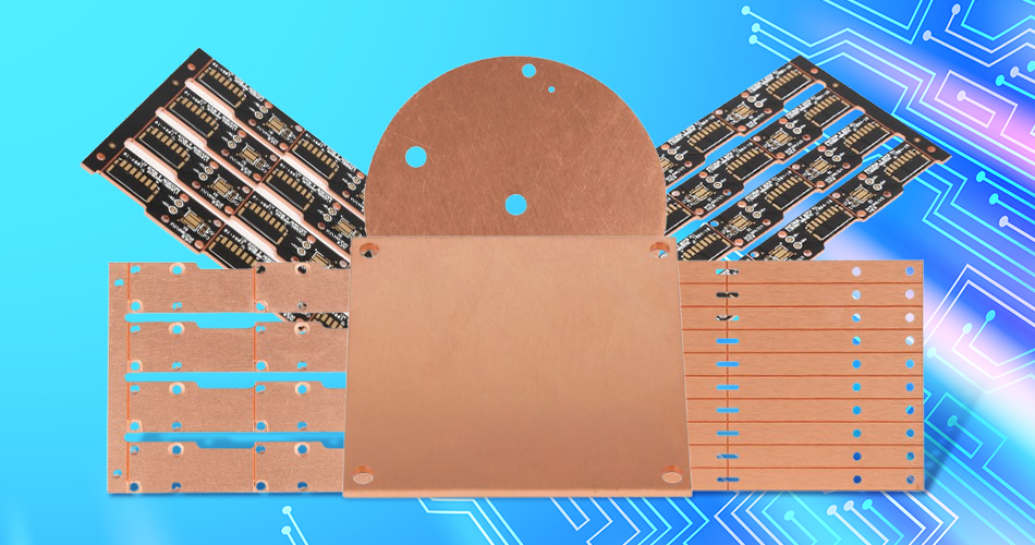
The sinkpad’s metal core and via metallization must be compatible to ensure mechanical reliability and thermal efficiency. Copper vias are commonly used for their high conductivity, paired with aluminum or copper sinkpads to maximize heat transfer. For high-temperature RF applications, copper-tungsten (CuW) sinkpads offer superior thermal stability, while compatible via metallization prevents galvanic corrosion. Conductive or resin via filling may be employed to improve thermal contact between the sinkpad and inner layers, enhancing heat spreading without introducing additional signal loss.

RF Application Sinkpad Vias PCB is tailored to address the unique demands of key high-frequency sectors, where environmental conditions and performance requirements vary significantly.
Satellite terminals operate in extreme temperature ranges and require exceptional signal sensitivity to detect weak RF signals. Sinkpad vias PCBs in these systems use radiation-hardened substrates and sinkpads with corrosion-resistant finishes to withstand cosmic radiation and temperature cycling. Blind/buried vias minimize signal path length, while ground via arrays reduce EMI, ensuring reliable communication with minimal signal loss. The sinkpad’s thermal management capabilities prevent overheating of power-hungry transceivers in sealed, weight-constrained satellite modules.
Radar systems and 5G base stations operate at high power levels and require rapid heat dissipation to maintain performance. Sinkpad vias PCBs here feature dense thermal via clusters under power amplifiers, channeling heat to the sinkpad core for efficient dissipation. Low-loss substrates minimize signal degradation in high-frequency radar bands, while optimized via placement reduces phase distortion critical for target detection. In 5G infrastructure, the sinkpad’s shielding properties reduce interference between closely packed RF components, supporting high-density deployments.
Aerospace RF systems demand ruggedness, lightweight design, and resistance to vibration and extreme temperatures. Sinkpad vias PCBs utilize lightweight aluminum sinkpads and flexible substrate sections to accommodate mechanical stress, while blind vias save space for compact avionics. The integration of sinkpad ground planes enhances EMI shielding, protecting sensitive RF circuits from external interference in mission-critical applications such as navigation and communication systems.

Successful RF Application Sinkpad Vias PCB implementation requires simulation-driven design—using 3D electromagnetic tools to model via parasitic effects and thermal performance before fabrication. Manufacturers employ precision drilling for blind/buried vias and strict quality control to ensure via alignment and sinkpad continuity. Collaborating with PCB fabricators early in the design process helps balance RF performance, thermal efficiency, and manufacturability, avoiding costly rework.
The future of RF Application Sinkpad Vias PCB lies in miniaturization and smart integration. Advancements in additive manufacturing enable complex via geometries and conformal sinkpad structures, optimizing both thermal and RF performance. Embedded sensors within sinkpads provide real-time thermal monitoring, enabling predictive maintenance for critical RF systems. Additionally, sustainable low-loss substrates and recyclable sinkpad materials align with industry efforts to reduce environmental impact without compromising performance.

RF Application Sinkpad Vias PCB represents a specialized solution that bridges the gap between thermal management and signal integrity in high-frequency systems. By integrating optimized via configurations with sinkpad technology, designers address the unique challenges of RF applications—mitigating parasitic effects, managing heat, and suppressing EMI—while meeting the demands of extreme environments. From satellite communication to 5G infrastructure, this technology enables the reliable, high-performance operation of next-generation RF systems. As frequency requirements continue to rise and form factors shrink, RF Application Sinkpad Vias PCB will remain a critical enabler, driving innovation through the seamless integration of thermal and RF design principles.

Got project ready to assembly? Contact us: info@apollopcb.com


We're not around but we still want to hear from you! Leave us a note:

Leave Message to APOLLOPCB
