


-
- PCB TYPE
- PRINTED CIRCUIT BOARD PROTOTYPE ALUMINUM PRINTED CIRCUIT BOARD R&F PCB FPC HIGH FREQUENCY PCB HIGH-TG PCB HEAVY COPPER PCB HDI PCB PCB FOR LIGHTING METAL CORE PCB

time:Aug 24. 2021, 16:48:54
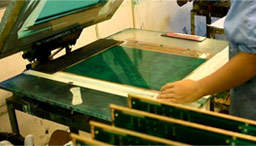
Generally speaking, PCB circuit board design is based on the circuit schematic diagram to achieve the purpose and function required by the circuit designer. Of course, such PCB circuit board design also requires the designer's years of experience accumulation, then the circuit board How does the factory produce high-quality products? I think there are the following aspects.
1. Design of electric strata
Generally speaking, Shenzhen circuit board factory with good reputation and excellent service will design its electric ground layer as a power supply in the form of flower pads. The ground layer is opposite to the image on the actual printed board. All connections will be isolated lines. By the way, when drawing several sets of power or ground isolation lines, you should be careful not to leave gaps, otherwise it will cause two sets of power supplies to short-circuit, and of course the connected area should not be blocked.
2. Overlapping technology of pads in circuit board factories
The overlap of the pads represents the overlap of the holes. During the drilling process, Shenzhen PCB Factory will break the drill bit due to multiple drilling in the same place, resulting in damage to the hole. Therefore, which product of the Shenzhen PCB factory is better, then the overlap of its holes has been inspected layer by layer.
Three, surface mount device pad technology
Surface mount device pad technology is for continuity testing. For very dense surface mount devices, the distance between his feet is very small, and his pads are also exceptionally thin. When installing test pins At the time, the positions must be staggered up and down, so as to ensure the high quality of the circuit board to a high degree. For the circuit board company that has passed the quality certification, his surface mount device pads are not too short.

Got project ready to assembly? Contact us: info@apollopcb.com


 Whatsapp 0086 755 29438407
 Mail info@apollopcb.com
 Tel 0086 755 29438407


ABOUT US

PRODUCTS
TECHNOLOGY
KNOWLEDGE CENTRE
CULTURE
NEWS
We're not around but we still want to hear from you! Leave us a note:

Leave Message to APOLLOPCB
