-
- PCB TYPE
- PRINTED CIRCUIT BOARD PROTOTYPE ALUMINUM PRINTED CIRCUIT BOARD R&F PCB FPC HIGH FREQUENCY PCB HIGH-TG PCB HEAVY COPPER PCB HDI PCB PCB FOR LIGHTING METAL CORE PCB
time:Nov 03. 2025, 11:58:05
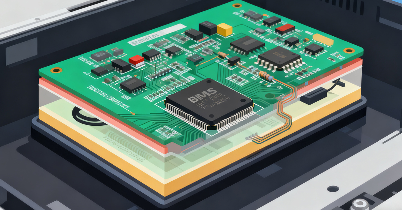
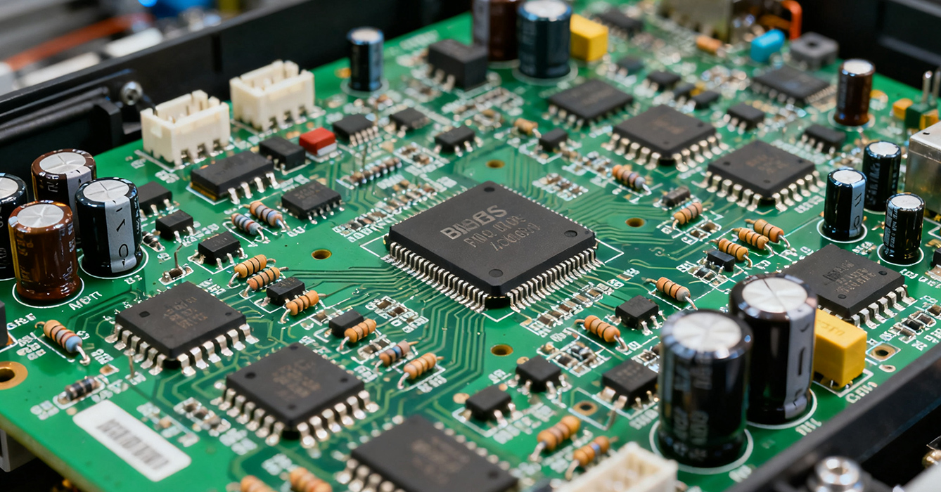
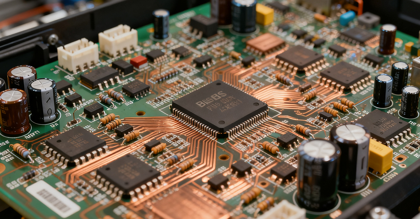
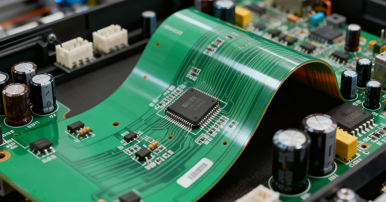
PCB Assembly is the critical bridge between printed circuit board (PCB) design and functional electronic devices, encompassing the integration of components—from resistors and capacitors to advanced semiconductors—onto PCBs. As the backbone of electronics manufacturing, this process balances precision, efficiency, and reliability to meet the demands of diverse sectors, from medical devices to telecommunications. Unlike PCB fabrication (which focuses on creating the bare board), PCB assembly transforms empty substrates into operational circuits, requiring mastery of both traditional and cutting-edge techniques. This article explores the foundational processes of PCB assembly, its tailored adaptations across industries, key quality control measures, and emerging trends shaping its evolution.
PCB assembly follows a structured workflow, with each step designed to ensure component integrity and electrical performance:
- Design for Assembly (DFA) Validation: Before production, engineers review PCB designs to optimize for assembly—simplifying component placement, ensuring adequate spacing for tools, and standardizing part sizes to reduce complexity. This pre-production step minimizes rework and improves yield.
- Component Preparation & Inspection: Components are sourced, verified against bill of materials (BOM) specifications, and prepared (e.g., trimming leads for through-hole components, verifying tape-and-reel packaging for surface-mount parts). Automated component counters and visual inspection prevent faulty or incorrect parts from entering the line.
- Hybrid Assembly (SMT + THT): Most modern PCBs use a mix of surface-mount technology (SMT) and through-hole technology (THT). SMT components are placed via automated pick-and-place machines and soldered in reflow ovens, while THT parts (often for high-power or mechanical stability) are inserted manually or via automated insertion machines and wave-soldered.
- Post-Assembly Finishing & Testing: Assembled PCBs undergo cleaning to remove flux residues, then testing—including in-circuit testing (ICT) to check component connectivity, functional testing to validate operational performance, and visual inspection (AOI) to detect soldering defects like bridging or tombstoning.

Medical devices (e.g., pacemakers, diagnostic scanners) require PCB assembly that adheres to strict sterility, reliability, and regulatory standards (ISO 13485). Assemblies use biocompatible materials, undergo rigorous traceability documentation, and often include conformal coating to protect against moisture and chemical exposure in clinical environments.
5G base stations and network equipment demand PCB assemblies with high signal integrity and thermal efficiency. Assembly processes prioritize controlled-impedance routing, low-loss solder materials, and heat-dissipating techniques (e.g., thermal pads, heat sinks) to handle the high-frequency, high-power demands of 5G technology.
Solar inverters and wind turbine controllers rely on PCB assemblies that withstand extreme outdoor conditions. Assembly adaptations include using UV-resistant conformal coatings, corrosion-resistant component finishes, and vibration-dampening mounting to ensure longevity in harsh environments like deserts or offshore wind farms.

Implementing barcode or RFID tracking for components and assemblies enables end-to-end traceability, critical for recalling faulty parts and complying with industry regulations. Cloud-based BOM management systems update in real time, reducing errors from outdated component data.
Automating repetitive tasks—such as component placement, solder paste inspection (SPI), and AOI—improves consistency and reduces human error. Collaborative robots (cobots) assist with THT insertion and manual assembly tasks, enhancing efficiency without sacrificing precision.
Proactive measures like statistical process control (SPC) monitor assembly parameters (e.g., reflow temperature, solder paste volume) to detect deviations early. Root-cause analysis tools (e.g., fishbone diagrams) address recurring defects, such as solder voids or component misalignment, at their source.

PCB assembly is evolving to meet the needs of next-generation electronics, with key trends including AI-driven process control (machine learning algorithms predict defects and optimize parameters), miniaturization with micro-assembly (handling components as small as 01005 size), and sustainable manufacturing (using lead-free solders, recyclable flux, and energy-efficient equipment to reduce environmental impact).

PCB Assembly is an indispensable part of electronics manufacturing, requiring a blend of technical expertise, industry-specific adaptation, and continuous optimization. By focusing on foundational processes, rigorous quality control, and emerging technologies, manufacturers can produce PCBs that meet the reliability and performance demands of modern devices. As electronics grow more complex—driven by 5G, IoT, and renewable energy—PCB assembly will remain a dynamic field, adapting to new challenges and enabling innovation across sectors.

Got project ready to assembly? Contact us: info@apollopcb.com


We're not around but we still want to hear from you! Leave us a note:

Leave Message to APOLLOPCB
