-
- PCB TYPE
- PRINTED CIRCUIT BOARD PROTOTYPE ALUMINUM PRINTED CIRCUIT BOARD R&F PCB FPC HIGH FREQUENCY PCB HIGH-TG PCB HEAVY COPPER PCB HDI PCB PCB FOR LIGHTING METAL CORE PCB
time:Oct 14. 2025, 09:50:58
Printed Circuit Boards (PCBs) are at the heart of nearly every electronic device. But how do these critical components come to life? The process of turning a blank board into a functioning PCB involves several intricate steps. In this article, we’ll break down the PCB assembly process, making it simple and easy to understand.
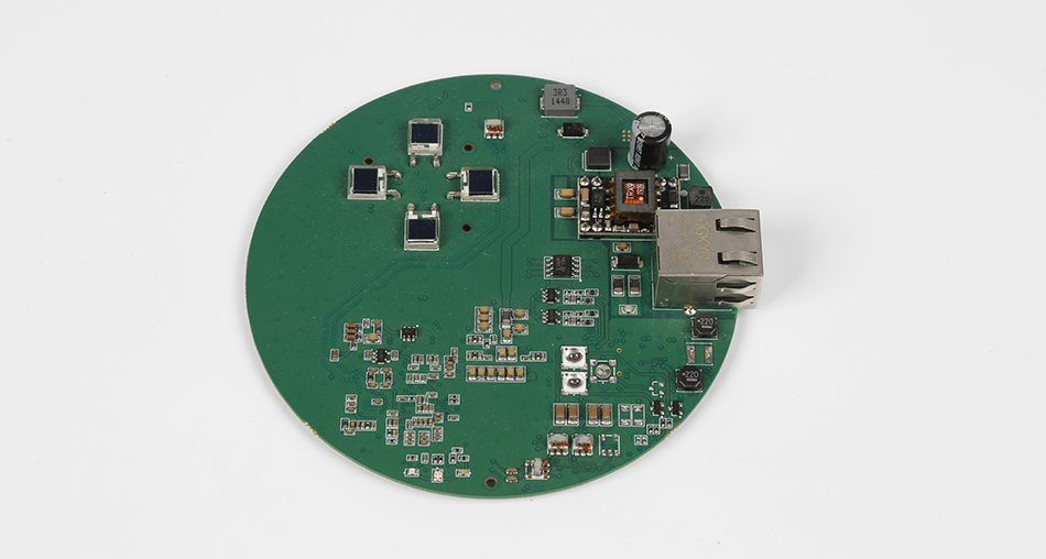
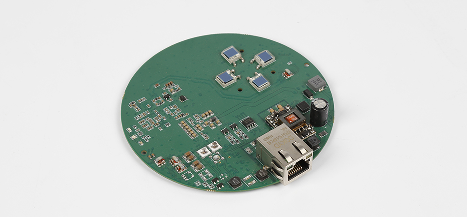
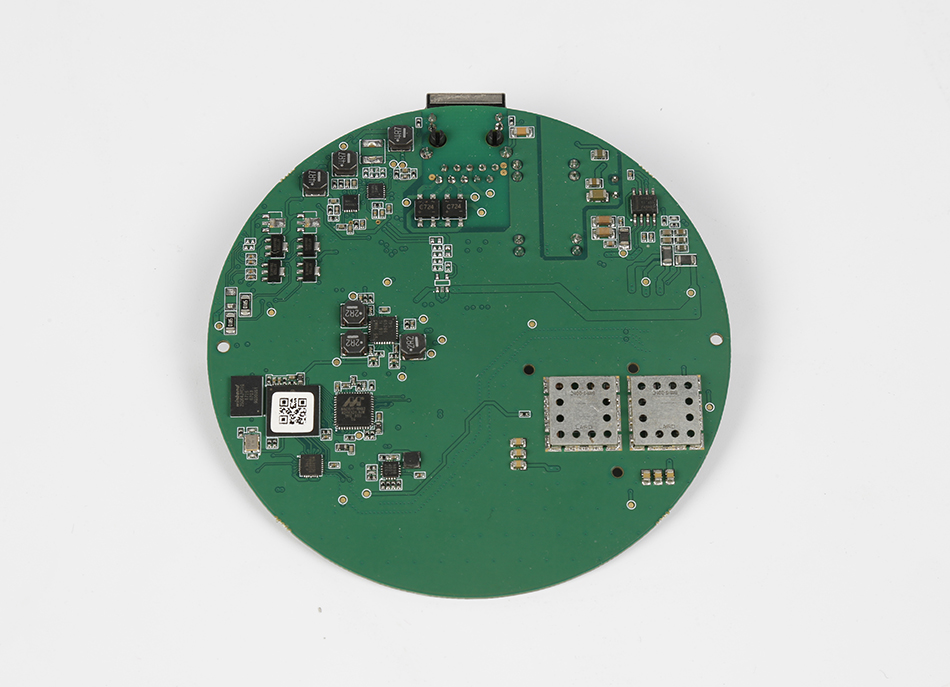
PCB assembly is the process of attaching electronic components to a printed circuit board. This process turns the basic board into a working circuit that can perform a specific function. There are various stages involved, from design to testing, ensuring that the final product is ready for use.

The first step in the PCB assembly process is designing the board. PCB design involves creating a layout that specifies where each component will be placed and how they will be connected. This design is typically done using specialized software that allows engineers to create detailed schematics and layouts.
A well-thought-out design is crucial because it ensures the board will function as intended. During this phase, engineers must consider the size of the components, the layout of the circuitry, and the overall purpose of the board. Mistakes in this stage can lead to significant issues later on.
Once the design is finalized, it's time to apply solder paste to the board. Solder paste is a mixture of tiny solder balls and flux, which helps the solder melt and bond to the components. This paste is applied to the areas where components will be mounted.
A stencil is used to apply solder paste precisely to the desired areas. The stencil has openings that match the locations where components will be placed. The paste is spread over the stencil, and the excess is removed, leaving paste only in the necessary spots.
With solder paste in place, the next step is placing the components on the board. This task is usually performed by automated machines known as pick-and-place machines. These machines rapidly and accurately position components on the board.
The Role of Pick-and-Place Machines
Pick-and-place machines use vacuum nozzles to pick up components and place them onto the board. They are programmed to follow the design layout, ensuring each component is correctly positioned. This automation speeds up the process and reduces the risk of human error.
Once the components are placed, the board goes through a soldering process to secure the components permanently. There are two main soldering techniques: reflow soldering and wave soldering.
Reflow Soldering
In reflow soldering, the board is heated in an oven. The heat causes the solder paste to melt, forming a strong bond between the components and the board. This method is typically used for surface-mounted components.
Wave Soldering
For boards with through-hole components, wave soldering is used. The board passes over a wave of molten solder, which adheres to the exposed metallic areas and creates electrical connections.

After soldering, the board undergoes thorough inspection to ensure all components are correctly placed and securely attached. Various methods are employed to check the quality of the assembly.
Types of Inspection
by Maria Luisa del Carmen Romero Centeno (https://unsplash.com/@luisaromero)
Visual Inspection: This is often the first step, where experts visually examine the board for obvious defects.
Automated Optical Inspection (AOI): This uses cameras to scan the board for defects such as missing components or misalignment.
X-ray Inspection: This is used to inspect solder joints that are not visible, such as those under large chips.
Even after thorough inspections, testing is essential to ensure the PCB functions as expected. Various tests are conducted, such as:
In-Circuit Testing (ICT): Checks the functionality of individual components.
Functional Testing: Simulates the board's working environment to ensure it performs its intended functions.
Once the PCBs pass all inspections and tests, they move to the final assembly phase. This step involves integrating the PCB into its final product, whether it's a smartphone, computer, or any other electronic device.

The PCB assembly process is a fascinating blend of design, precision, and technology. By understanding each step, from design to final assembly, you can appreciate the complexity and skill involved in creating these essential components. Whether you're a hobbyist or a professional in the electronics industry, knowing the intricacies of PCB assembly can enhance your understanding and appreciation of modern electronics.

Got project ready to assembly? Contact us: info@apollopcb.com


We're not around but we still want to hear from you! Leave us a note:

Leave Message to APOLLOPCB
