-
- PCB TYPE
- PRINTED CIRCUIT BOARD PROTOTYPE ALUMINUM PRINTED CIRCUIT BOARD R&F PCB FPC HIGH FREQUENCY PCB HIGH-TG PCB HEAVY COPPER PCB HDI PCB PCB FOR LIGHTING METAL CORE PCB
time:Oct 23. 2025, 17:55:16
Printed Circuit Boards, or PCBs, are essential components in almost every electronic device we use today. From smartphones to washing machines, they form the backbone of electronic circuits. But how do these intricate boards come to life? Understanding the PCB assembly process is key to appreciating how our modern devices function.
PCB assembly is the process of connecting electronic components to the printed circuit board. This involves a series of steps that transform a blank board into a functional piece of technology. It's a critical phase in the manufacturing of electronic devices.
Before diving into the assembly process, it’s important to understand the role of PCB design. A well-thought-out design ensures that the board can efficiently support and connect electronic components. This involves creating a schematic that outlines the electrical connections and laying out the physical design of the board.
Effective PCB design can prevent potential issues during assembly and improve the overall functionality and reliability of the device.
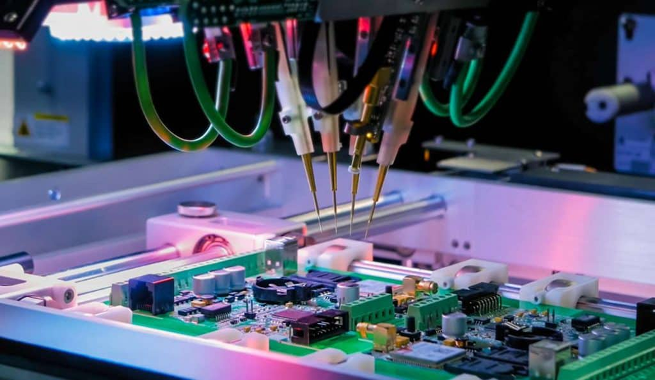
The PCB assembly process involves several key steps, each crucial to the successful production of a working circuit board.
The first step in the PCB assembly process is applying solder paste to the board. Solder paste is a mixture of tiny solder balls and flux. It's applied to the areas of the board where components will be attached, typically using a stencil and a squeegee to ensure precision.
Once the solder paste is applied, it's time to place the components on the board. This is often done using a pick-and-place machine, which accurately positions the components on the board. The machine is programmed to know exactly where each component should go, based on the PCB design.
After the components are placed, the next step is to secure them to the board through soldering. There are two main methods for soldering in PCB assembly:
Reflow Soldering: This method involves passing the board through an oven. The heat melts the solder paste, creating a solid connection between the components and the board.
Wave Soldering: Used for through-hole components, the board is passed over a wave of molten solder, which adheres to the exposed metal and forms connections.
Quality control is vital in the PCB assembly process. After soldering, the boards are inspected to ensure that the components are correctly placed and the connections are solid. This can be done manually or through automated optical inspection (AOI), which uses cameras to quickly identify any issues.
Testing is a crucial step that ensures the PCB functions as intended. Various tests can be conducted, such as:
In-Circuit Testing (ICT): Verifies the functionality of the circuit by testing individual components.
Functional Testing: Assesses whether the board performs its intended functions in real-world conditions.
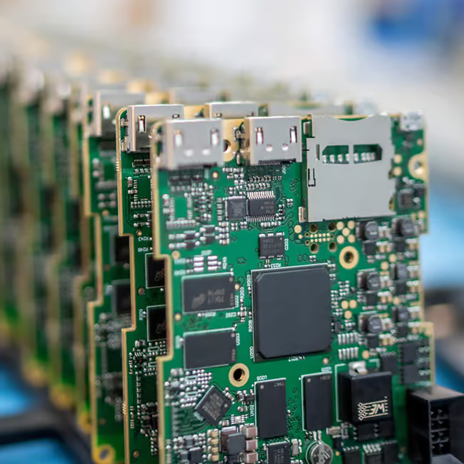
PCB manufacturing is the process of producing the physical boards before assembly. This involves several steps, including:
Fabrication: Creating the board layers and drilling holes.
Etching: Removing excess copper to reveal circuit patterns.
Laminating: Bonding layers together to form a single board.
Manufacturing lays the foundation for assembly, ensuring that the boards are ready to receive components and function correctly.
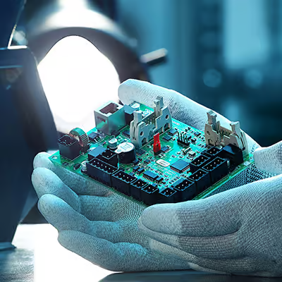
PCB assembly is not without its challenges. Here are some common issues:
Component Misalignment: Incorrect placement can lead to poor connections or functional failures.
Soldering Defects: Issues like solder bridges or voids can cause short circuits or weak connections.
Design Flaws: Poor PCB design can complicate assembly and result in non-functional boards.
Addressing these challenges involves careful planning, precise execution, and thorough testing throughout the assembly process.
With advancements in technology, the PCB assembly process is continually evolving. Automation and machine learning are being increasingly integrated, improving precision and efficiency. Additionally, new materials and techniques are emerging, allowing for more compact and complex designs.
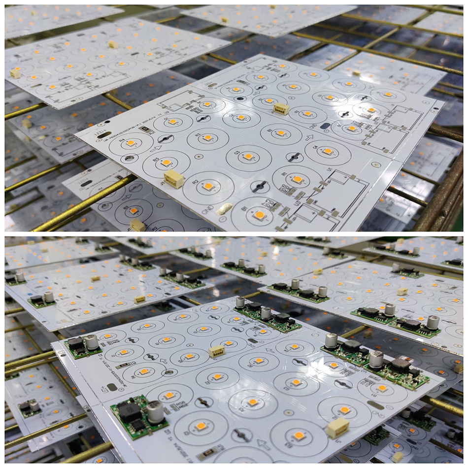
Understanding the PCB assembly process provides valuable insights into how electronic devices are brought to life. From design and manufacturing to assembly and testing, each step is crucial in creating reliable and functional circuit boards. As technology progresses, the PCB assembly process will continue to innovate, driving the development of even more sophisticated electronic devices.
By familiarizing yourself with the intricacies of PCB assembly, you gain a deeper appreciation for the technology that powers our world. Whether you're a hobbyist, engineer, or simply curious, knowing how PCBs are assembled can enhance your understanding of electronics and the devices we rely on daily.
Got project ready to assembly? Contact us: info@apollopcb.com


We're not around but we still want to hear from you! Leave us a note:

Leave Message to APOLLOPCB
