-
- PCB TYPE
- PRINTED CIRCUIT BOARD PROTOTYPE ALUMINUM PRINTED CIRCUIT BOARD R&F PCB FPC HIGH FREQUENCY PCB HIGH-TG PCB HEAVY COPPER PCB HDI PCB PCB FOR LIGHTING METAL CORE PCB
time:Sep 03. 2025, 14:34:49
China has established itself as a dominant force in the electronics manufacturing industry, becoming synonymous with high-volume production and rapid innovation. The country's extensive infrastructure, skilled workforce, and technological advancements have made it an ideal locati0n for PCB production, attracting companies from around the globe. China's ability to deliver competitive pricing, high-quality standards, and fast turnaround times has solidified its reputation as a premier destination for PCB manufacturing. As businesses continue to seek efficiency and excellence in their production processes, China remains at the forefront, driving innovation and setting new standards in the industry.
Chinese PCB manufacturers offer several compelling advantages that make them the preferred choice for businesses worldwide.
Cost Efficiency: One of the most significant benefits is cost efficiency. Chinese manufacturers can provide competitive pricing due to economies of scale and lower labor costs, which are pivotal for companies looking to maximize their budget without compromising on quality. This affordability is complemented by a streamlined supply chain that reduces overhead expenses and enhances overall cost savings.
Advanced Technology: Many Chinese PCB manufacturers have invested heavily in state-of-the-art equipment and technology, ensuring they remain competitive on the global stage. This commitment to technological advancement enables them to produce complex and high-performance PCBs that meet the diverse needs of various industries, from consumer electronics to automotive and aerospace applications.
Skilled Workforce: The availability of experienced engineers and technicians in China ensures high-quality production and innovation. These skilled professionals are adept at navigating the complexities of PCB design and fabrication, bringing precision and expertise to every project. Their ability to troubleshoot and optimize production processes is a key factor in maintaining the high standards expected by international clients.
Scalability: Whether you need a small batch or large-scale production, Chinese manufacturers can accommodate your needs with remarkable flexibility. This scalability is crucial for businesses that experience fluctuating demands or are in the process of scaling their operations. Chinese manufacturers can quickly adjust production volumes to meet market requirements, providing a significant advantage in dynamic industries.
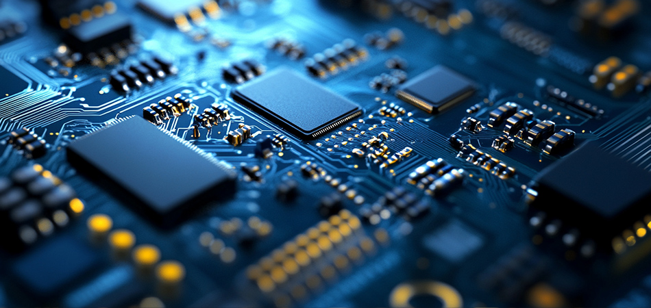
PCB manufacturing is a complex process that involves several intricate steps, each contributing to the final product's functionality and reliability. Understanding these stages will help you appreciate the intricacies of PCB fabrication in China and the meticulous attention to detail required at each phase.
Before production begins, a PCB design is created using specialized software. This design includes the layout, component placement, and electrical pathways, ensuring the board meets the necessary specifications and performance criteria. The design phase is critical, as any errors or oversights can lead to costly revisions or functional failures down the line. Once the design is finalized, a prototype is produced to test functionality and performance. Prototyping is an essential step that allows for the identification and correction of potential issues before full-scale production commences. It provides an opportunity to refine the design, optimize component placement, and ensure the board's overall reliability.
Choosing the right materials is crucial for the performance and durability of a PCB. Common materials include fiberglass, copper, and solder mask, each serving a specific function in the board's construction. The choice of materials can significantly impact the board's thermal management, electrical conductivity, and mechanical strength. In China, manufacturers have access to a wide range of materials, allowing for customized solutions based on specific requirements. This access to diverse materials enables manufacturers to tailor their offerings to meet the unique needs of their clients, whether it involves enhancing heat dissipation, improving signal integrity, or achieving specific aesthetic goals.
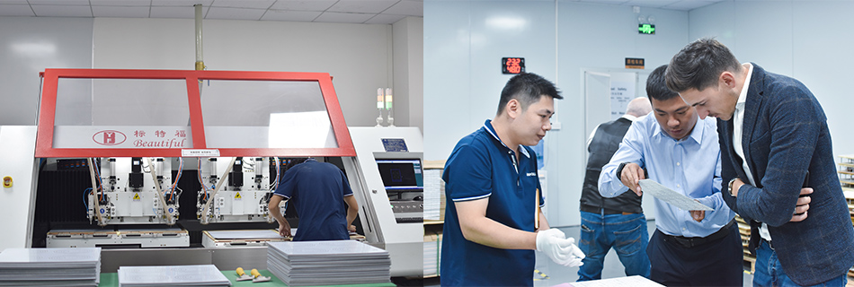
Most PCBs consist of multiple layers, each serving a distinct purpose within the board's architecture. The layering process involves bonding sheets of copper to a substrate, creating the foundation for the electrical circuits. Then, a photoresist layer is applied to the copper, and the board is exposed to light to transfer the circuit design onto the board. This imaging process is critical for defining the intricate patterns that make up the board's circuitry. Precision in layering and imaging is essential to ensure that the final product meets the required specifications and performs reliably under various conditions.
The next step is etching, which removes excess copper, leaving behind the desired circuit pattern. This process involves using chemical solutions to dissolve unwanted copper, revealing the precise pathways that enable electrical connectivity. Following etching, plating is performed, where a thin layer of metal, such as gold or silver, is applied to the copper traces. Plating improves conductivity, enhances solderability, and prevents oxidation, ensuring the board's long-term reliability and performance. The choice of plating material can also influence the board's overall cost and compatibility with specific applications.
Holes are drilled into the PCB to create vias, which are used to connect different layers of the board. Precision drilling is vital to ensure electrical connectivity and structural integrity, as any misalignment or errors can compromise the board's functionality. Advanced drilling techniques and equipment are employed to achieve the necessary accuracy, accommodating the increasingly complex designs demanded by modern electronics. The creation of vias allows for seamless communication between different layers, enabling the integration of multiple functions within a single board.
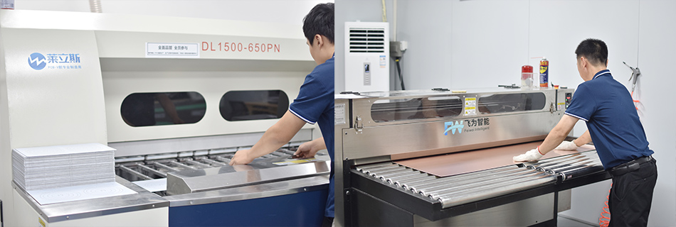
A solder mask is applied to protect the copper traces from oxidation and to prevent solder bridges during component placement. The mask is typically green, but other colors are available based on aesthetic preferences and specific application requirements. The application of the solder mask is a critical step in ensuring the board's durability and reliability, as it provides an additional layer of protection against environmental factors and mechanical wear. The choice of solder mask color can also serve functional purposes, such as improving visibility during assembly or aligning with branding guidelines.
The surface finish protects the exposed copper and ensures reliable soldering. Common finishes include HASL (Hot Air Solder Leveling), ENIG (Electroless Nickel Immersion Gold), and OSP (Organic Solderability Preservatives). Each finish offers unique benefits and is chosen based on the specific requirements of the application, such as cost considerations, environmental conditions, and soldering techniques. The surface finish plays a crucial role in the board's performance, influencing its thermal characteristics, corrosion resistance, and overall longevity.
Once the PCB is fabricated, components are mounted onto the board. This process can be done manually or through automated machinery, depending on the complexity and volume of production. Automated assembly ensures precision and consistency, reducing the likelihood of errors and enhancing overall efficiency. Quality control checks are essential to ensure the board functions correctly and meets design specifications. These checks involve rigorous testing and inspection processes to identify any defects or inconsistencies before the PCBs are shipped to clients.
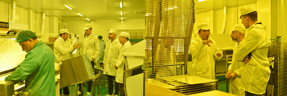
Chinese manufacturers adhere to strict quality standards to ensure reliable and high-performance PCBs. Many factories are certified with international standards such as ISO 9001, ISO 14001, and IPC-A-600. These certifications guarantee that manufacturers follow best practices in production and quality control, providing clients with the confidence that their products will meet or exceed industry standards.
Comprehensive testing and inspection processes are vital to catch any defects before the PCBs are shipped. Common tests include:
Electrical Testing: Verifies the electrical functionality of the board, ensuring that it performs as intended under various conditions.
X-ray Inspection: Checks for internal defects like voids or misaligned layers, which can compromise the board's structural integrity and performance.
AOI (Automated Optical Inspection): Inspects the board for surface defects and component placement accuracy, using advanced imaging technology to identify any discrepancies.
These testing and inspection procedures are integral to maintaining the high quality and reliability that clients expect from Chinese manufacturers. By employing cutting-edge technology and rigorous protocols, manufacturers can deliver PCBs that consistently meet the demanding requirements of modern electronics.
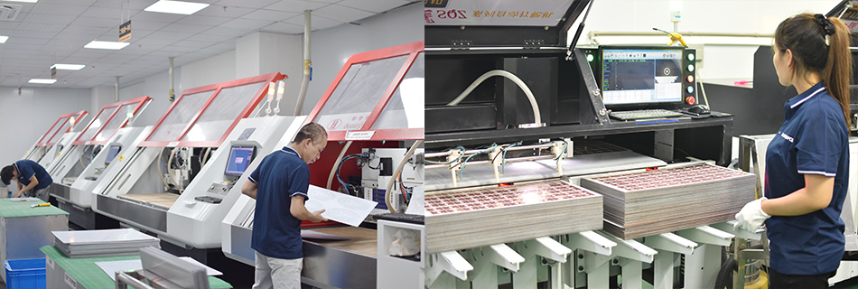
When selecting a PCB manufacturer in China, several factors should be considered to ensure a successful partnership and optimal results:
Reputation and Experience: Research the manufacturer's history and customer reviews to gauge their reliability and track record in delivering quality products. A reputable manufacturer with a proven history is more likely to meet your expectations and provide a positive experience.
Technological Capability: Ensure they have the necessary technology to meet your design specifications, particularly if your project involves complex or innovative designs. Manufacturers equipped with advanced technology are better positioned to handle challenging requirements and deliver exceptional results.
Communication and Support: Effective communication is crucial for successful project management, as it facilitates collaboration and ensures that both parties are aligned on objectives and expectations. Choose a manufacturer that offers strong support and is responsive to your needs and inquiries.
Lead Time: Confirm their ability to meet your production schedule, especially if you have tight deadlines or specific launch dates. A manufacturer's ability to deliver on time is essential for maintaining your project's timeline and achieving your business goals.
PCB manufacturing in China offers numerous advantages, from cost savings to high-quality production. By understanding the processes and considerations involved, you can make informed decisions and partner with the right manufacturer for your needs. Whether you're a startup or an established company, leveraging China's PCB manufacturing capabilities can help you bring your electronic products to market efficiently and effectively. The sophisticated and reliable nature of the PCB manufacturing process in China ensures that, with the right partner, you can achieve exceptional results and gain a competitive edge in the electronics industry. Embracing these opportunities can lead to innovative solutions and successful product launches, solidifying your position in the market and driving future growth.

Got project ready to assembly? Contact us: info@apollopcb.com


We're not around but we still want to hear from you! Leave us a note:

Leave Message to APOLLOPCB
