-
- PCB TYPE
- PRINTED CIRCUIT BOARD PROTOTYPE ALUMINUM PRINTED CIRCUIT BOARD R&F PCB FPC HIGH FREQUENCY PCB HIGH-TG PCB HEAVY COPPER PCB HDI PCB PCB FOR LIGHTING METAL CORE PCB
time:Oct 13. 2025, 14:46:23
Printed Circuit Boards (PCBs) are the backbone of almost all electronic devices today. From your smartphone to your laptop, PCBs are essential components. Understanding how these boards are manufactured can provide valuable insights into the world of electronics. In this article, we'll take you through the PCB manufacturing process in a straightforward way.

A PCB, or Printed Circuit Board, is a board used to mechanically support and electrically connect electronic components. The board uses conductive pathways, or traces, etched from copper sheets laminated onto a non-conductive substrate.
PCBs are crucial because they allow for compact and organized electronic assemblies. They eliminate the need for complex wiring, making electronic devices more reliable and easier to repair or upgrade.
The PCB manufacturing process is complex and involves several steps, each crucial to ensuring the final product is of high quality. Here's a detailed look at the process.
The first step in PCB manufacturing is the design phase. Engineers use specialized software to design the layout of the PCB. This design includes the placement of components and the routing of electrical connections.
Once the design is complete, it's printed onto a special film. This film serves as a template for the next stages of the manufacturing process.
The substrate is the base material of the PCB. It's typically made from fiberglass, which provides structural support. A layer of copper is then applied to both sides of the substrate.
In this step, the unnecessary copper is removed. The board is coated with a photoresist, and the design is transferred from the film to the board using UV light. The exposed areas are then etched away, leaving only the desired copper traces.
For multi-layer PCBs, this step involves aligning and bonding the layers together. Layers are precisely aligned and then pressed to form a single, solid board.
Next, holes are drilled into the board. These holes are used to mount electronic components and to create electrical connections between layers.
Once drilled, the board undergoes a plating process. A thin layer of copper is deposited inside the drilled holes, allowing for electrical connectivity between the layers.
A solder mask is applied to protect the copper traces from accidental contact and to prevent solder bridges during component assembly. The solder mask also gives the PCB its characteristic green color.
The silkscreen is used to print symbols and labels on the PCB for easier identification and assembly. This step adds the finishing touch to the board's appearance.
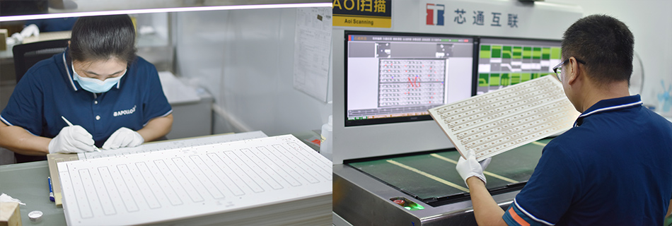
Before a PCB is ready for assembly, it undergoes rigorous testing to ensure there are no defects. This includes electrical tests to verify that all connections are functioning as intended.

Once the PCB is manufactured, the next step is PCB assembly, where components are mounted onto the board.
SMT is a method where components are mounted directly onto the surface of the PCB. This process is automated and allows for the assembly of highly complex PCBs with small components.
THT involves inserting component leads through the drilled holes on the PCB and soldering them in place. This method provides strong mechanical bonds and is often used for components that will experience physical stress.

EMS providers offer specialized services for the design, manufacturing, and assembly of electronic components and PCBs. They have the expertise and equipment to produce high-quality PCBs efficiently.
Expertise and Experience: EMS providers have specialized knowledge and experience in PCB manufacturing and assembly.
Cost-Effective: Outsourcing to EMS providers can be more cost-effective than maintaining in-house manufacturing capabilities.
Scalability: EMS providers can scale production to meet demand, making them ideal partners for businesses of all sizes.
Understanding the PCB manufacturing process offers valuable insights into the world of electronics. From design to assembly, each step is crucial in creating reliable and efficient electronic devices. By leveraging the expertise of EMS providers, businesses can ensure the production of high-quality PCBs that meet the demands of today's technology-driven world.
Whether you're an engineer, a hobbyist, or simply curious about how electronic devices are made, understanding PCBs is an essential part of understanding modern technology.

Got project ready to assembly? Contact us: info@apollopcb.com


We're not around but we still want to hear from you! Leave us a note:

Leave Message to APOLLOPCB
