-
- PCB TYPE
- PRINTED CIRCUIT BOARD PROTOTYPE ALUMINUM PRINTED CIRCUIT BOARD R&F PCB FPC HIGH FREQUENCY PCB HIGH-TG PCB HEAVY COPPER PCB HDI PCB PCB FOR LIGHTING METAL CORE PCB
time:Nov 13. 2025, 18:49:16
Thermoelectric Separation PCB Tech stands as a groundbreaking advancement in electronic packaging, solving the persistent conflict between thermal management and electrical performance in power-dense devices. Unlike traditional PCBs where thermal dissipation and signal transmission compete for the same conductive paths—resulting in compromised efficiency, signal distortion, or premature component failure—this innovative technology achieves thermal-electrical decoupling through purpose-built layer architecture. By channeling heat through dedicated metallic structures while confining electrical signals to isolated circuits, Thermoelectric Separation PCB Tech empowers high-performance components (e.g., high-power semiconductors, microwave modules, and EV power electronics) to operate at maximum capacity without thermal or electrical tradeoffs. This article delves into the latest technical innovations, comparative advantages over legacy systems, expanded industry applications, critical design imperatives, and future trajectories of this transformative PCB technology.

The next generation of thermoelectric separation PCBs builds on foundational principles with three cutting-edge advancements:
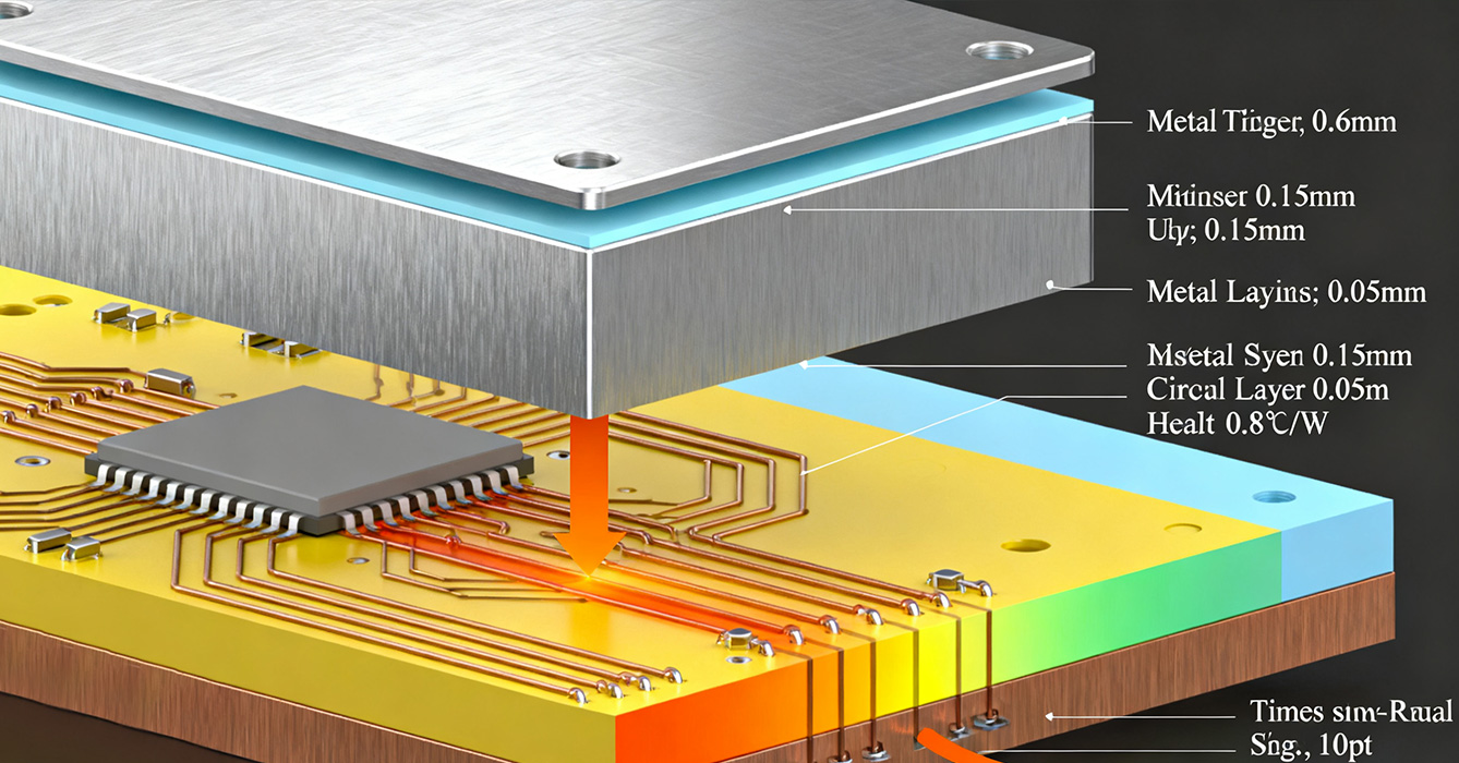
At the technology’s core is a thick, thermally optimized metal core—typically high-purity copper or aluminum alloy—engineered exclusively for heat conduction. This core acts as a "thermal backbone," directly interfacing with high-power components to rapidly absorb and disperse heat. Unlike conventional MCPCBs where the metal layer doubles as a ground plane, this thermal core is electrically isolated from signal layers via advanced dielectric materials, eliminating short-circuit risks while maximizing heat transfer efficiency.
A thin, high-performance dielectric layer—such as ceramic-polymer composites or nanomaterial-reinforced polyimide—separates the thermal core from electrical circuits. This film is engineered to deliver dual functionality: maintaining robust electrical insulation between the metal core and signal traces while facilitating efficient thermal conduction. Next-gen dielectric formulations minimize thermal resistance by up to 40% compared to standard materials, ensuring unobstructed heat flow from components to the thermal core.
Electrical signals are routed on independent copper layers (top, bottom, or inner layers) that are fully isolated from the thermal core. These layers support high-density routing, impedance-controlled traces, and high-current paths—all optimized for electrical performance without thermal constraints. This isolation enables engineers to design circuits for maximum signal integrity while the thermal core handles heat dissipation independently, eliminating the need for design compromises.

Thermoelectric Separation PCB Tech outperforms traditional PCBs and even standard MCPCBs with four distinct benefits:
By dedicating an entire layer to heat transfer, the technology cuts thermal resistance by 35–55% compared to FR-4 PCBs and 25–35% compared to conventional MCPCBs. This translates to cooler operating temperatures for high-power components, reducing thermal throttling and extending service life by 25–30% in harsh environments.
Electrical circuits are no longer constrained by thermal pathways, enabling optimized routing for high-frequency (GHz-range) and high-current signals. This eliminates crosstalk, voltage sag, and EMI issues caused by overlapping thermal and electrical paths—critical for applications like 5G base stations, radar systems, and precision power electronics.
Engineers can independently scale thermal and electrical performance: adjusting the thermal core thickness to match heat loads without altering circuit design, or optimizing signal traces for impedance control without restricting heat flow. This versatility streamlines product development, reducing prototype iterations by 30–40%.
Decoupling thermal and electrical paths eliminates thermal stress on solder joints, vias, and connectors—common failure points in legacy PCBs. The rigid metal core also enhances mechanical stability, reducing warpage and delamination during extreme temperature cycles (-50°C to 150°C) and vibration.

Thermoelectric Separation PCB Tech is driving innovation across four high-growth sectors:
Industrial power converters and renewable energy inverters use the technology to cool IGBTs, MOSFETs, and SiC/GaN semiconductors. The thermal core dissipates heat from these high-current components, enabling higher power densities and improving efficiency by 5–10% compared to traditional cooling solutions.
Satellite transceivers, 5G base station amplifiers, and radar modules rely on the technology’s signal-thermal isolation. The isolated circuit layers maintain signal integrity for high-frequency (1–100 GHz) operations, while the thermal core cools power amplifiers—enabling higher output power without signal distortion.
EV traction inverters, onboard chargers, and battery management systems (BMS) leverage the technology to handle high currents and extreme heat. The thermal core channels heat from power electronics to the vehicle’s cooling system, while isolated circuits ensure safe, reliable power distribution—critical for EV performance and safety.
High-power laser diodes and laser drivers use thermoelectric separation PCB Tech to maintain precise operating temperatures. The technology’s thermal efficiency and signal isolation enable stable laser output, reducing drift and extending diode life—essential for medical imaging, industrial cutting, and aerospace applications.
To maximize performance, engineers must address three key design considerations:
Choose dielectric films based on application requirements: ceramic-polymer composites for high-temperature (150°C+) environments, nanomaterial-reinforced polyimides for flexible or low-profile designs, and high-thermal-conductivity formulations for ultra-high-power applications.
Ensure uniform, high-integrity bonding between the thermal core and dielectric layer to prevent delamination. Advanced manufacturing processes like vacuum thermal compression bonding create a consistent bond line, minimizing thermal resistance and enhancing reliability.
Use high-performance TIMs (e.g., phase-change materials, graphene-based greases) or solderable pads to create a low-resistance connection between components and the thermal core. Avoid over-sizing component pads, as this can compromise electrical isolation.
The evolution of Thermoelectric Separation PCB Tech is shaped by three key trends:
Next-Gen Material Integration: Graphene-reinforced thermal cores and dielectric films are being developed to further reduce thermal resistance and weight, targeting aerospace and portable applications.
Smart Thermal Management: Embedded temperature sensors and AI-driven control systems will enable real-time thermal monitoring and dynamic cooling adjustment, optimizing performance for variable loads.
Additive Manufacturing: 3D-printed thermal cores with complex internal geometries (e.g., micro-channels, fractal heat spreaders) will enable customized heat paths for ultra-specific applications, maximizing thermal efficiency in minimal space.
Thermoelectric Separation PCB Tech represents a paradigm shift in electronic packaging, decoupling thermal and electrical performance to unlock new levels of efficiency, reliability, and design versatility. By leveraging specialized thermal cores, advanced dielectrics, and isolated circuits, the technology outperforms legacy PCBs in high-power, high-performance applications—from EV electronics to 5G communications. As electronics continue to push toward higher power density and miniaturization, Thermoelectric Separation PCB Tech will remain a critical enabler of innovation, proving that separating thermal and electrical pathways is the key to unlocking next-gen device performance.

Got project ready to assembly? Contact us: info@apollopcb.com


We're not around but we still want to hear from you! Leave us a note:

Leave Message to APOLLOPCB
