-
- PCB TYPE
- PRINTED CIRCUIT BOARD PROTOTYPE ALUMINUM PRINTED CIRCUIT BOARD R&F PCB FPC HIGH FREQUENCY PCB HIGH-TG PCB HEAVY COPPER PCB HDI PCB PCB FOR LIGHTING METAL CORE PCB
time:Sep 12. 2025, 11:47:27
In the world of electronics, printed circuit boards (PCBs) are the backbone of most modern devices. These boards connect various electronic components, allowing them to communicate and function together. One of the advanced techniques in PCB design is the use of HDI (High-Density Interconnect) technology, specifically the incorporation of blind and buried vias. In this article, we will explore the significance of HDI blind buried vias, the process of manufacturing these PCBs, and the factors to consider when choosing an HDI blind buried vias PCB maker.
PCB design is the art and science of creating a layout for the electronic components that make up a circuit. The design must be precise and efficient to ensure the circuit functions as intended. HDI technology is a cutting-edge advancement in PCB design that allows for a higher density of components on the board. This is achieved through the use of smaller vias, finer lines and spaces, and thinner materials. HDI technology makes it possible to fit more components in a smaller area, which is crucial for modern electronics that demand compact and powerful solutions.
Vias are small holes that are drilled into PCBs to allow electrical connections between different layers of the board. There are three main types of vias:
Through-Hole Vias: These are the most common type of vias that go through the entire board.
Blind Vias: These connect the outer layer of the board to one or more inner layers but do not go through the entire board.
Buried Vias: These are located entirely within the inner layers of the board and do not reach the outer layers.
Blind and buried vias are essential for HDI PCBs because they allow for more complex designs without increasing the size of the board. They enable designers to create multi-layered boards with intricate pathways, enhancing the functionality of the device.

The manufacturing of HDI blind buried vias PCBs is a sophisticated process that requires precision and attention to detail. Here is an overview of the steps involved:
The first step is designing the PCB layout using specialized software. The design must account for the placement of all components, the routing of electrical connections, and the integration of blind and buried vias. The design must be meticulously planned to ensure efficiency and functionality.
Once the design is finalized, the layers of the PCB are stacked together. The stacking process involves laminating the layers to create a single, cohesive board. This step is crucial as it determines the overall structure and integrity of the PCB.
The next step is drilling the vias. Advanced machinery is used to drill precise holes for the blind and buried vias. The accuracy of this process is vital, as any errors can compromise the functionality of the PCB.
After drilling, the vias are plated with a conductive material, usually copper. This process is known as electroplating and is essential for establishing electrical connections between the layers of the board.
The PCB is then etched to create the desired circuit patterns. After etching, a solder mask is applied to protect the board from environmental damage and to prevent solder bridges during component assembly.
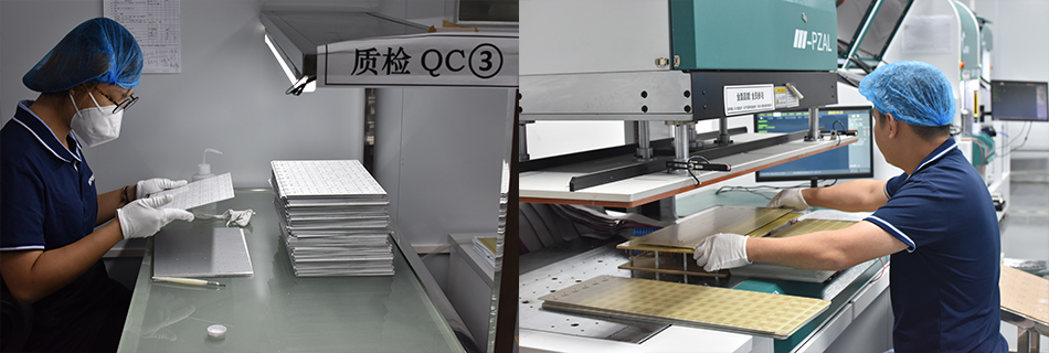
Finally, the PCB undergoes rigorous testing to ensure it meets the required specifications and functions correctly. Quality assurance is a critical step to guarantee the reliability and performance of the PCB.

Selecting the right PCB maker is crucial to the success of your electronic project. Here are some factors to consider when choosing an HDI blind buried vias PCB manufacturer:
Look for a manufacturer with extensive experience and expertise in HDI PCB design and manufacturing. An experienced maker will have a proven track record of producing high-quality PCBs and will be able to offer valuable insights and guidance throughout the process.
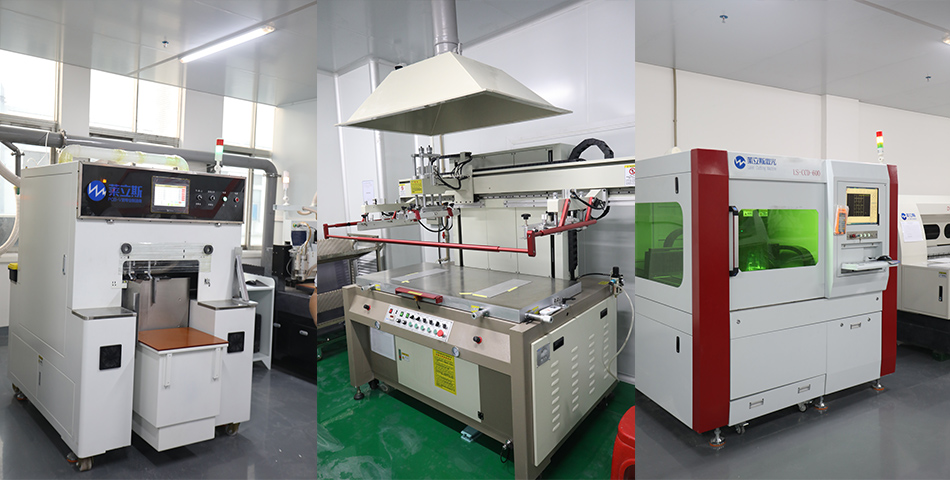
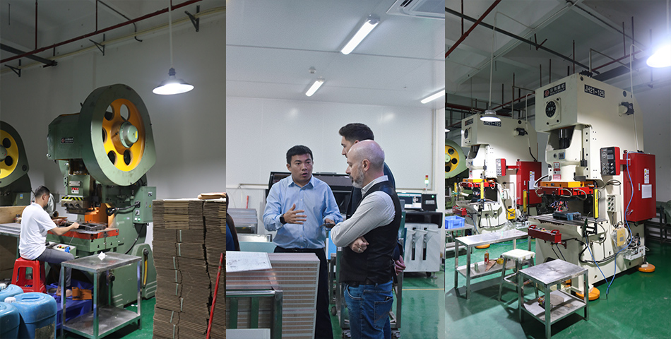
Ensure that the manufacturer uses the latest technology and equipment for PCB production. Advanced machinery and techniques are essential for achieving the precision and accuracy required for HDI blind buried vias PCBs.
A reliable manufacturer will have strict quality control measures in place to ensure the consistency and reliability of their products. Inquire about their testing and inspection processes to ensure that they meet industry standards.
Choose a manufacturer that offers customization options to meet your specific requirements. Whether you need a unique design or specific materials, a flexible maker will be able to accommodate your needs.
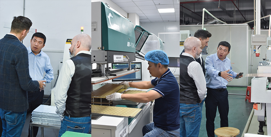
Effective communication and support are vital for a successful partnership. Select a manufacturer that values customer service and is responsive to your inquiries and concerns.

HDI blind buried vias PCBs represent the pinnacle of modern PCB design, enabling the creation of compact, high-performance electronic devices. Understanding the intricacies of HDI technology and the manufacturing process is essential for making informed decisions about your PCB needs. By choosing the right HDI blind buried vias PCB maker, you can ensure the success of your project and the reliability of your electronic products. Whether you're developing consumer electronics, industrial equipment, or cutting-edge technology, the right PCB partner will help you bring your vision to life.


Got project ready to assembly? Contact us: info@apollopcb.com


We're not around but we still want to hear from you! Leave us a note:

Leave Message to APOLLOPCB
