-
- PCB TYPE
- PRINTED CIRCUIT BOARD PROTOTYPE ALUMINUM PRINTED CIRCUIT BOARD R&F PCB FPC HIGH FREQUENCY PCB HIGH-TG PCB HEAVY COPPER PCB HDI PCB PCB FOR LIGHTING METAL CORE PCB
time:Jul 05. 2025, 10:13:04
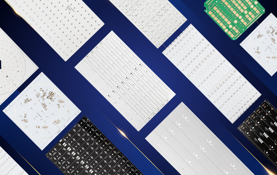
In the intricate realm of printed circuit boards (PCBs), the selection of substrate material significantly impacts electronic devices' performance, reliability, and functionality. Among available options, aluminum base PCB substrates have gained prominence, particularly those with a thickness like 1.6mm. This specific thickness balances mechanical strength, thermal management, and design flexibility, fitting diverse industrial applications. This article delves into aluminum base PCB substrates, covering material traits, design aspects, manufacturing, quality control, applications, and market trends.
Material Characteristics of Aluminum Base PCB Substrates
Aluminum Alloy Selection
The performance of an aluminum base PCB substrate hinges on the chosen aluminum alloy. Aluminum alloys combine high thermal conductivity, good mechanical strength, and corrosion resistance, key for PCB substrates.
Pure aluminum alloys, such as the 1xxx series, are prized for excellent thermal conductivity, ideal for applications prioritizing heat dissipation. However, they have lower mechanical strength compared to alloyed aluminum. Alloyed aluminum, like the 6xxx series with magnesium and silicon, offers enhanced strength while maintaining good thermal conductivity. These alloys withstand mechanical stresses and vibrations during PCB operation and have improved corrosion resistance, making them suitable for various environments.
Dielectric Layer Properties
The dielectric layer in aluminum base PCB substrates serves dual purposes: electrical insulation and heat transfer facilitation. Choosing the right dielectric material is crucial for PCB performance optimization.
Polyimide - based dielectrics are favored for high - temperature and high - frequency applications due to their excellent thermal stability and low dielectric loss. This makes them suitable for 5G devices, radar systems, and high - performance computing. Ceramic - filled epoxies, combining good electrical insulation with enhanced thermal conductivity, are cost - effective and widely used in consumer electronics, LED lighting, and industrial control systems.
Copper Layer Considerations
High - purity copper is standard for conductive layers in aluminum base PCB substrates because of its low electrical resistance, ensuring efficient power delivery and minimizing power losses. Copper layer thickness is determined by circuit current - carrying needs, with thicker layers used for high - current applications. Surface treatments like ENIG, ENEPIG, or OSP protect copper from oxidation, improve solderability, and enhance PCB reliability in harsh environments.
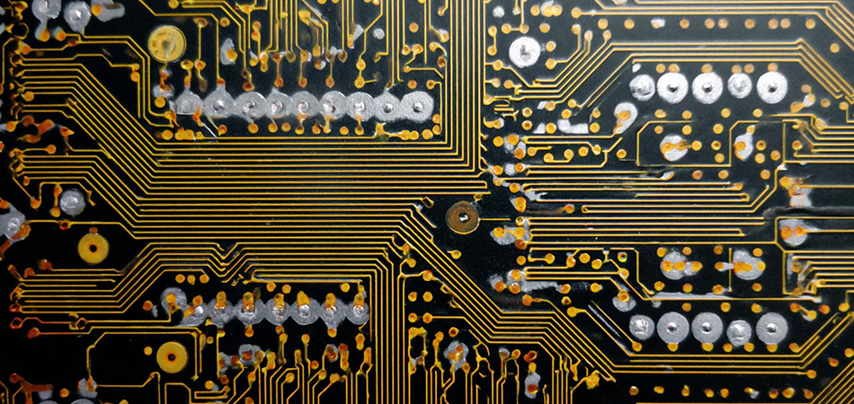
Design Considerations for Aluminum Base PCB Substrates
Thermal Management Design
Aluminum base PCB substrates excel in heat management, with thermal vias playing a crucial role. These vias connect surface copper layers to the aluminum substrate, facilitating heat transfer. Optimizing their size, number, and distribution based on component heat - generating characteristics is essential. Combining thermal vias with heat sinks or spreaders further boosts thermal performance by increasing heat exchange surface area.
Electrical Design
Electrical design is vital for aluminum base PCB substrates, especially in high - speed and high - frequency applications. Maintaining signal integrity requires proper trace routing, impedance control, and shielding. For power - intensive circuits, efficient power distribution, minimizing voltage drops and EMI, and isolating power domains are key. Multi - layer designs separate power and signal layers to reduce crosstalk.
Mechanical Design
The 1.6mm - thick aluminum base PCB substrates offer decent mechanical strength, but additional measures may be needed in some scenarios. Stiffeners or supports can enhance rigidity in large or vibration - prone PCBs. Careful design of mounting and fastening methods ensures secure attachment while minimizing stress transmission to the PCB.
Environmental Considerations
Aluminum base PCB substrates are used in diverse environments, some harsh. Conformal coatings protect against moisture, dust, and chemicals, with material choice depending on application requirements. Additionally, proper enclosure design provides ventilation and environmental protection.
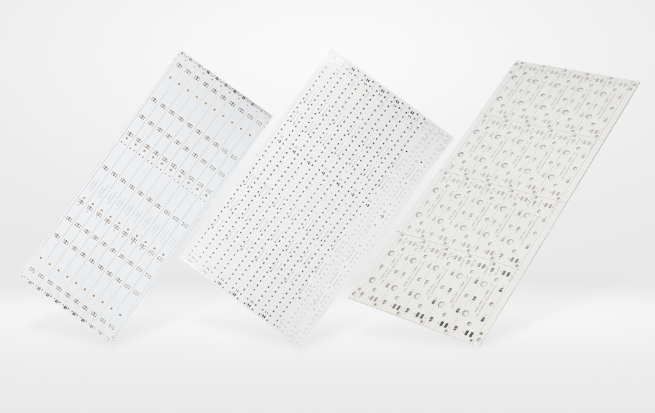
Manufacturing Processes of Aluminum Base PCB Substrates
Drilling
Two main methods are used for drilling in aluminum base PCB substrates: mechanical and laser drilling. Mechanical drilling is cost - effective for larger holes but may cause issues like drill bit wear and burr formation. Laser drilling offers high precision, ideal for small, complex holes in HDI PCBs, though it is more expensive.
Plating
The plating process, involving electroless and electrolytic plating, deposits copper for electrical conductivity. Electroless plating coats non - conductive surfaces first, followed by electrolytic plating to build up the copper layer. Advanced techniques like pulse plating can improve copper layer quality.
Lamination
High - pressure lamination bonds the aluminum substrate, dielectric layer, and copper layers using adhesive films or prepregs. Proper lamination is crucial for structural integrity, electrical performance, and thermal conductivity, preventing delamination and ensuring efficient heat transfer.
Surface Finishing
Surface finishing protects copper traces and prepares them for soldering. HASL is a traditional, cost - effective option. OSP is suitable for fine - pitch components and environmentally friendly. ENIG offers excellent corrosion resistance and a smooth surface, ideal for high - reliability applications.
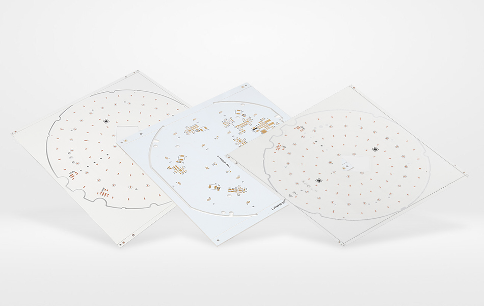
Quality Assurance for Aluminum Base PCB Substrates
Incoming Material Inspection
Before manufacturing, all incoming materials, including the aluminum substrate, copper foil, dielectric materials, and components, are rigorously inspected. Checks include flatness, purity, alloy composition, and mechanical properties of the aluminum substrate, among others, to ensure only high - quality materials are used.
In - Process Quality Control
During manufacturing, quality control is maintained at every stage. Drilled holes are inspected for accuracy, plating thickness and uniformity are monitored, lamination is checked for proper bonding, and surface finishing is evaluated for defects. AOI systems detect issues early for timely correction.
Final Testing
Completed PCBs undergo comprehensive final testing. Electrical tests check for short circuits, open circuits, and impedance matching. Thermal tests, like thermal cycling and infrared thermography, assess thermal management, and mechanical tests evaluate strength and durability.
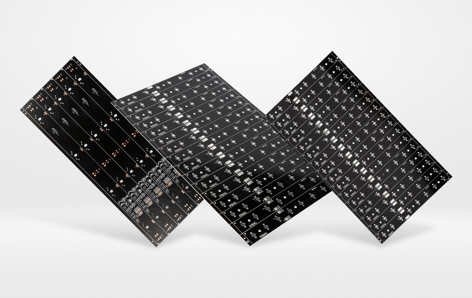
Applications of Aluminum Base PCB Substrates
LED Lighting
LED lighting is a major application area for aluminum base PCB substrates. Their thermal conductivity and appropriate thickness effectively manage LED heat, ensuring performance and lifespan. They are used in various lighting products, from residential fixtures to large - scale architectural lighting, with customizable features.
Automotive Electronics
In the automotive industry, these substrates are increasingly used in electronic systems like power inverters and ADAS. They offer thermal management, mechanical strength, and environmental resistance, ensuring reliable operation and enhancing vehicle safety and efficiency.
Industrial Electronics
Industrial electronics rely on aluminum base PCB substrates to withstand harsh conditions while managing component heat. Their strength and conductivity support power - intensive applications, ensuring continuous industrial equipment operation.
Consumer Electronics
With the demand for high - performance consumer devices rising, these substrates help dissipate heat from components, improving device performance and lifespan. Their thin and lightweight nature suits modern consumer electronics design.
Aerospace and Defense
In aerospace and defense, aluminum base PCB substrates are used in critical applications. They withstand extreme conditions, ensuring the proper functioning of electronic systems essential for mission success and personnel safety.
Market Analysis of Aluminum Base PCB Substrates
Market Size and Growth
The global market for aluminum base PCB substrates has been growing steadily and is expected to continue. The demand for high - performance electronics and efficient heat management drives this growth, with new technologies like 5G and IoT creating more opportunities.
Regional Analysis
The market is geographically diverse. Asia - Pacific, led by China, is the largest market due to its manufacturing base and growing electronics industries. North America and Europe are important for high - end applications, while the Middle East, Africa, and Latin America are emerging markets with increasing electronics investment.
Competitive Landscape
The market is highly competitive, with companies focusing on product quality, innovation, cost - effectiveness, and customer service. Some target niche markets, while others aim at mass - market applications. New entrants with novel technologies intensify competition and drive innovation.
In conclusion, aluminum base PCB substrates, especially those with a 1.6mm thickness, are indispensable in the electronics industry. As electronics evolve towards miniaturization and higher performance, demand for these substrates will surge. Continued R&D efforts will focus on enhancing thermal conductivity, reducing weight, and improving insulation. Manufacturers must meet growing demand while maintaining quality, controlling costs, and adhering to environmental regulations. Collaboration among different sectors will be key to overcoming challenges and driving future innovation in this field.

Got project ready to assembly? Contact us: info@apollopcb.com


We're not around but we still want to hear from you! Leave us a note:

Leave Message to APOLLOPCB
