-
- PCB TYPE
- PRINTED CIRCUIT BOARD PROTOTYPE ALUMINUM PRINTED CIRCUIT BOARD R&F PCB FPC HIGH FREQUENCY PCB HIGH-TG PCB HEAVY COPPER PCB HDI PCB PCB FOR LIGHTING METAL CORE PCB
time:Nov 18. 2025, 13:57:16
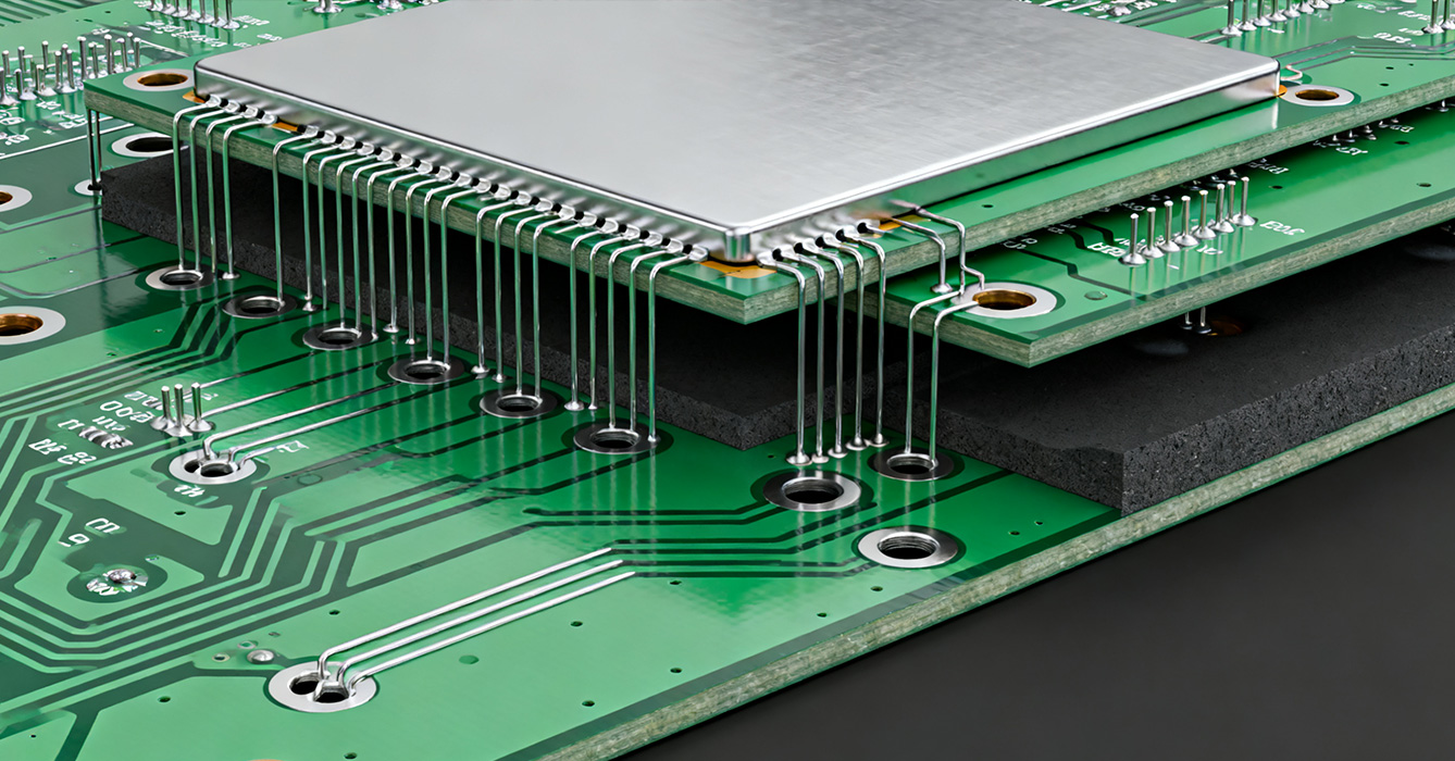
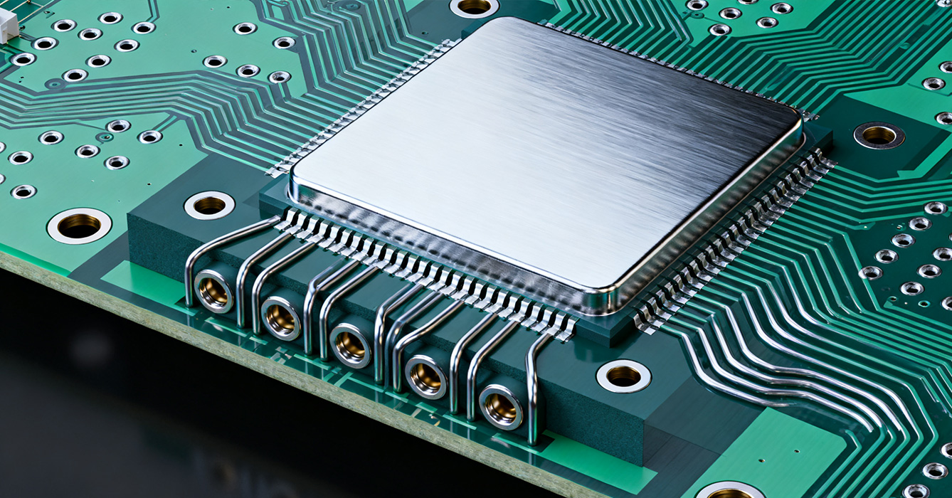
Blind and Buried Vias Sinkpad PCB has emerged as a transformative solution for modern electronic systems, addressing the conflicting demands of high-density interconnects (HDI) and efficient thermal management. By combining blind/buried via technology— which eliminates unnecessary through-hole penetration—with sinkpad structures that enhance heat dissipation, this specialized PCB design empowers the miniaturization and performance enhancement of electronic devices. As industries ranging from AI terminals and AR/VR to edge computing push for smaller form factors, higher component densities, and increased power efficiency, Blind and Buried Vias Sinkpad PCB has become indispensable. This article explores the design synergies, manufacturing considerations, application innovations, and future trends that define this advanced PCB technology, highlighting its role in resolving thermal-electrical tradeoffs in next-generation electronics.
The core advantage of Blind and Buried Vias Sinkpad PCB lies in its ability to integrate three critical requirements: high 布线密度 (routing density), unobstructed thermal flow, and robust signal integrity—without mutual compromise.
Blind vias (connecting surface layers to inner layers) and buried vias (linking inner layers exclusively) eliminate the space-wasting penetration of traditional through-holes, enabling tighter component placement and more efficient use of PCB real estate. This optimization is particularly impactful for compact devices, where every millimeter of space matters. When paired with sinkpads, these vias are strategically routed around the metal core to avoid disrupting thermal pathways. Designers leverage the sinkpad’s continuous metal structure as a reference plane, aligning blind/buried vias to maximize routing channels while preserving the sinkpad’s ability to spread heat. This synergy allows for significantly higher component densities compared to standard PCBs, supporting the integration of complex circuits in AI chips, AR/VR sensors, and edge computing modules.
Sinkpads rely on unbroken metal cores to conduct heat away from high-power components, and blind/buried vias are engineered to complement this function. Unlike through-holes, which can create thermal barriers by piercing the sinkpad core, blind/buried vias are confined to specific layers, maintaining the sinkpad’s structural and thermal integrity. Thermal vias—implemented as blind or buried configurations—are clustered near heat-generating components, channeling thermal energy directly to the sinkpad core for dissipation. This targeted thermal routing ensures that high-density interconnects do not compromise heat transfer, a critical consideration for power-hungry devices like AI accelerators and compact computing modules.
Blind and buried vias minimize signal path length and reduce parasitic effects compared to through-holes, as they avoid unnecessary layer crossings. When integrated with sinkpads, the metal core acts as a stable ground reference, suppressing crosstalk and electromagnetic interference (EMI) in dense routing environments. By eliminating via stubs and reducing impedance discontinuities, this design ensures reliable signal transmission even at high frequencies—essential for data-intensive applications like AI server communication and AR/VR data processing. The sinkpad’s shielding properties further enhance signal integrity by confining electromagnetic energy, preventing interference between adjacent high-speed signals.

Producing Blind and Buried Vias Sinkpad PCB requires precision manufacturing processes to balance via quality, sinkpad integrity, and thermal-electrical performance.
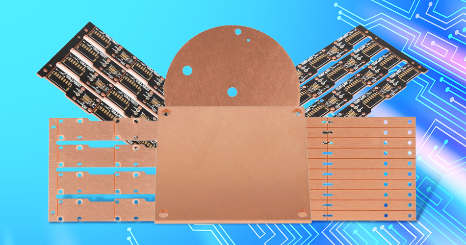
Blind and buried vias demand advanced drilling techniques, such as laser drilling, to achieve accurate layer targeting without damaging the sinkpad core. Manufacturers must ensure strict alignment between vias and sinkpad structures, as misalignment can create thermal bottlenecks or signal disruptions. Electroplating processes are optimized to ensure uniform via metallization, enhancing both electrical conductivity and thermal transfer. For sinkpads made of aluminum or copper, compatibility between via materials and the metal core is critical to prevent galvanic corrosion and maintain long-term reliability. Post-drilling processes, such as resin filling, may be employed to reinforce vias and improve thermal contact with the sinkpad.
The manufacturing process must preserve the sinkpad’s thermal conductivity while accommodating blind/buried vias. This involves careful control of material removal during via drilling to avoid thinning the sinkpad core excessively. For high-temperature applications, manufacturers may use copper-tungsten (CuW) sinkpads paired with gold-plated blind vias to enhance thermal stability and corrosion resistance. Quality control measures, including X-ray inspection and thermal imaging, verify via alignment, sinkpad continuity, and thermal performance, ensuring that the final product meets stringent industry standards.

Blind and Buried Vias Sinkpad PCB is driving innovation in industries where compact size, high performance, and thermal efficiency are paramount.
The proliferation of AI-enabled devices—from smartphones to edge computing nodes—demands high-density PCBs that can handle increased power loads. Blind and Buried Vias Sinkpad PCB supports the integration of AI chips with dense interconnects while managing the heat generated by NPU (Neural Processing Unit) operations. This design enables the miniaturization of AI terminals without sacrificing computational power, making it a key enabler for portable AI applications and high-performance AI servers.
AR/VR headsets and wearables require ultra-compact, lightweight PCBs with high component density to support sensors, displays, and processing units. Blind and buried vias maximize routing space in these small form factors, while sinkpads dissipate heat from power-hungry components like microprocessors and wireless modules. This combination ensures reliable performance in sealed, space-constrained AR/VR devices, where overheating can degrade user experience or cause component failure.
Edge computing modules operate in harsh industrial environments, requiring rugged PCBs that balance density, thermal efficiency, and durability. Blind and Buried Vias Sinkpad PCB enables the integration of multiple high-speed interfaces (Ethernet, PCIe) and processing components in compact, vibration-resistant designs. The sinkpad’s thermal management capabilities protect sensitive electronics from extreme temperature fluctuations, while blind/buried vias support the high data rates needed for real-time industrial processing.

The evolution of Blind and Buried Vias Sinkpad PCB is shaped by the growing demands of AI, IoT, and wearable technology, with three key trends emerging:
Advancements in AI-driven PCB design tools are enabling automated optimization of blind/buried via placement and sinkpad routing. These tools simulate thermal flow, signal integrity, and routing density simultaneously, reducing design cycles and improving performance. Machine learning algorithms can predict potential thermal-electrical conflicts, allowing designers to refine layouts before fabrication.
The industry is moving toward sustainable substrate materials and recyclable sinkpad cores, aligning with global environmental goals. Additionally, the adoption of graphene-enhanced substrates and advanced composites is improving thermal conductivity and reducing weight, further enhancing the performance of Blind and Buried Vias Sinkpad PCB in portable and energy-efficient devices.
As devices become increasingly compact and flexible, Blind and Buried Vias Sinkpad PCB is evolving to support conformal and flexible form factors. Additive manufacturing techniques are enabling the production of complex, 3D-shaped PCBs with integrated blind/buried vias and sinkpads, opening new possibilities for wearable electronics and embedded systems.

Blind and Buried Vias Sinkpad PCB represents a critical innovation in resolving the thermal-electrical tradeoffs that limit modern electronic systems. By combining high-density interconnects with efficient thermal management, this technology enables the miniaturization, performance enhancement, and reliability of devices across AI, AR/VR, edge computing, and industrial sectors. Its design synergies—balancing density, thermal flow, and signal integrity—address the core challenges of next-generation electronics, while ongoing advancements in manufacturing and materials promise even greater capabilities. As the demand for compact, high-performance electronics continues to grow, Blind and Buried Vias Sinkpad PCB will remain a cornerstone technology, driving innovation and enabling the development of more powerful, efficient, and portable devices.

Got project ready to assembly? Contact us: info@apollopcb.com


We're not around but we still want to hear from you! Leave us a note:

Leave Message to APOLLOPCB
