-
- PCB TYPE
- PRINTED CIRCUIT BOARD PROTOTYPE ALUMINUM PRINTED CIRCUIT BOARD R&F PCB FPC HIGH FREQUENCY PCB HIGH-TG PCB HEAVY COPPER PCB HDI PCB PCB FOR LIGHTING METAL CORE PCB
time:Sep 17. 2025, 10:01:18
In the world of printed circuit boards (PCBs), the demand for higher speed and better performance is constantly pushing the boundaries of design and manufacturing. One technique that has become increasingly important in this pursuit is back drilling. But what exactly is back drilling, and why is it so crucial in PCB design?
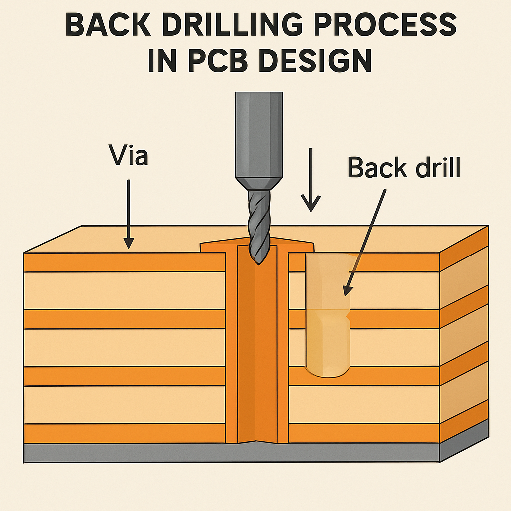
Back drilling is a process used in PCB manufacturing to remove unused portions of copper vias. Vias are tiny holes that allow electrical connections between different layers of a PCB. However, not all parts of a via are always necessary for making these connections. The unused segments, known as "stubs," can cause issues in high-speed PCBs by introducing signal integrity problems. Back drilling eliminates these stubs, thus enhancing the performance of the PCB.
The process involves drilling into the PCB from the opposite side of the original via hole, hence the term "back drilling." This is done precisely to remove the stub without affecting the necessary conductive path. By doing so, it reduces the potential for signal distortion and interference, which are critical factors in high-speed applications.

In high-speed PCB designs, maintaining signal integrity is paramount. The presence of via stubs can lead to reflections and impedance mismatches, which degrade signal quality. By removing these stubs through back drilling, designers can minimize such issues, ensuring that signals travel cleanly and efficiently across the board.
As devices become faster and more complex, the circuits that drive them must keep up. High-speed PCBs are essential for applications like telecommunications, data centers, and advanced computing. Back drilling helps to optimize these boards for speed by eliminating unnecessary copper that can slow down or distort signals.
Electromagnetic interference is another challenge in PCB design. Via stubs can act as antennas, unintentionally radiating electromagnetic waves that interfere with other components. Back drilling reduces these stubs, thereby decreasing the potential for EMI and improving the overall electromagnetic compatibility of the PCB.

The process starts during the design phase. Engineers must identify which vias require back drilling based on their locati0n and function in the circuit. The PCB design software is used to plan these drill points accurately, ensuring that the drilling will not compromise the structural integrity of the board.
During manufacturing, precision is key. Specialized drilling equipment is used to perform the back drilling process. The drill must be aligned perfectly to remove only the unwanted stub without damaging the rest of the via. This requires careful control of the drill depth and speed.
After back drilling, thorough inspections are conducted to ensure the process has been successful. This includes checking for any leftover stubs, ensuring there is no damage to the vias, and verifying that the electrical properties of the board meet the required specifications.
Improved Signal Quality: By removing via stubs, back drilling enhances the quality of signals, which is critical for high-speed PCBs.
Increased Reliability: With fewer potential points of failure, back-drilled PCBs tend to be more reliable in demanding applications.
Reduced EMI: The process helps in minimizing electromagnetic interference, which is essential for compliance with industry standards.
Increased Manufacturing Complexity: Back drilling adds an extra step to the manufacturing process, requiring specialized equipment and expertise.
Cost Considerations: The additional time and resources required for back drilling can increase the overall cost of PCB production.
Design Limitations: Not all PCB designs can accommodate back drilling, and careful planning is necessary to implement it effectively.

In the telecommunications industry, where high-speed data transmission is crucial, back drilling is often employed to ensure that PCBs can handle the demands of modern communication systems without signal degradation.
Data centers require PCBs that can manage vast amounts of data quickly and efficiently. Back drilling helps in achieving the necessary speed and reliability, making it a common practice in data center hardware.
In aerospace and defense applications, the reliability and performance of PCBs are critical. Back drilling contributes to the robustness and efficiency of these systems, supporting advanced technologies used in this sector.
Back drilling is an essential technique in the modern PCB manufacturing process, especially for high-speed applications. By removing unwanted via stubs, it enhances signal integrity, reduces electromagnetic interference, and improves overall performance. While it introduces some complexities and costs, the benefits it provides in terms of reliability and efficiency make it a valuable tool in the PCB designer's arsenal. As technology continues to evolve, techniques like back drilling will remain crucial in meeting the ever-increasing demands of electronic systems.
Understanding and implementing back drilling in PCB design can significantly impact the success of your high-speed applications, ensuring that your products perform at their best in today's competitive market.

Got project ready to assembly? Contact us: info@apollopcb.com


We're not around but we still want to hear from you! Leave us a note:

Leave Message to APOLLOPCB
