-
- PCB TYPE
- PRINTED CIRCUIT BOARD PROTOTYPE ALUMINUM PRINTED CIRCUIT BOARD R&F PCB FPC HIGH FREQUENCY PCB HIGH-TG PCB HEAVY COPPER PCB HDI PCB PCB FOR LIGHTING METAL CORE PCB
time:Aug 30. 2025, 15:03:10
CEM3 PCBis a versatile, cost-effective substrate for diverse electronics, bridging basic CEM1 PCBs (limited to low-demand uses) and high-cost specialized substrates (e.g., high-frequency FR4, ceramic) overengineered for mid-tier needs. It balances three key attributes: mechanical resilience for harsh conditions, stable dielectric performance for reliable signal transmission, and cost efficiency for mid-volume production—making it essential for industrial automation controllers, new energy charging equipment, and household appliances.
Manufacturers often struggle to find substrates that meet industry-specific performance without exceeding budgets: CEM1 fails in harsh environments (vibration, moisture), while specialized options strain mass-production costs. CEM3 solves this with adaptive features—enhanced thermal cycling resistance, optimized mixed-signal dielectric behavior, and compatibility with diverse assembly processes—tailored to distinct industry needs.
This article explores CEM3’s cross-industry performance upgrades, adaptation to new energy/5G industrial devices, design strategies to maximize value, and future trends—providing insights for engineers and procurement teams building reliable, scalable systems.
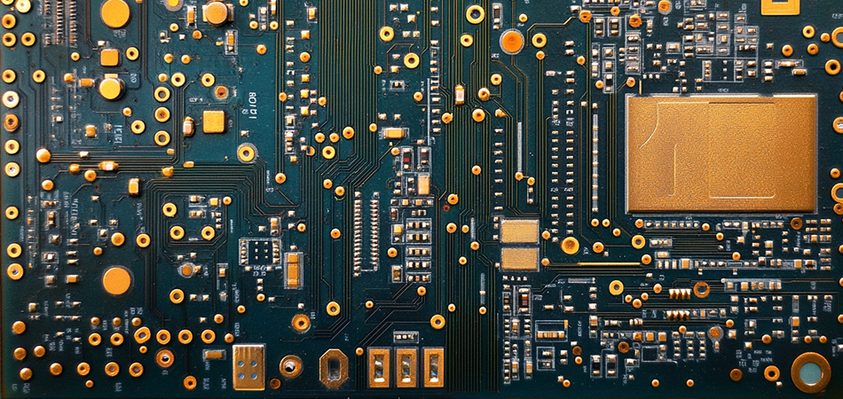
CEM3’s cross-industry appeal comes from three key performance upgrades over basic substrates, addressing mid-tier electronic pain points through intentional engineering.
Unlike CEM1 (prone to cracking/delamination), CEM3 withstands industrial, outdoor, and mobile application stress:
-Flexural Strength & Impact Resistance: Its epoxy-glass fiber matrix handles bending (e.g., portable sensors) without trace damage—maintaining integrity after 1,000 flex cycles (15mm radius) vs. CEM1’s 300-cycle failure.
Vibration & Shock Resistance: Strong interlayer adhesion prevents delamination in high-vibration settings (industrial machinery, new energy vehicle/NEV chargers). A CEM3-based factory conveyor controller survived 10,000 hours of 10–500 Hz vibration (no performance loss), while CEM1 failed at 4,500 hours.
Dimensional Stability: Low X-Y axis CTE minimizes warping in temperature swings—critical for precision systems (industrial sensors), where 0.1mm warping disrupts component alignment.
Systems integrating analog sensors and digital modules (industrial IoT gateways, smart home controllers) need consistent dielectric properties—CEM3 delivers this:
Controlled Dielectric Constant (Dk): Tightly regulated Dk (±2% variation) ensures reliable transmission for low-speed analog (temperature data) and moderate-speed digital (Wi-Fi 6) signals, reducing reflection/cross-talk vs. CEM1’s inconsistent Dk.
Low Dielectric Loss (Df): Df <0.02 at 1 MHz minimizes signal attenuation for long traces (e.g., industrial Ethernet controllers). A CEM3 gateway maintained 98% signal integrity over 10-meter traces vs. 85% for CEM1.
Insulation Resistance Stability: Moisture-resistant resin retains >10¹³ Ω·cm insulation in humid environments (outdoor smart meters), preventing leakage currents that corrupt data or cause shutdowns.
Specialized substrates (ceramic, metal-core FR4) are too expensive for 5,000–50,000 unit/year production—CEM3 balances performance and cost:
Low Material/Manufacturing Costs: Uses readily available epoxy/glass fiber and standard PCB lines (no specialized equipment), cutting per-unit costs 30–40% vs. high-end substrates.
High Production Yields: Consistent quality and automated assembly compatibility (pick-and-place, reflow soldering) yield >95%, reducing scrap. A smart thermostat maker reported 15% less scrap after switching from CEM1.
Fewer Design Iterations: Predictable mechanical/dielectric performance matches simulations, cutting design time 25% for an industrial sensor maker vs. CEM1.
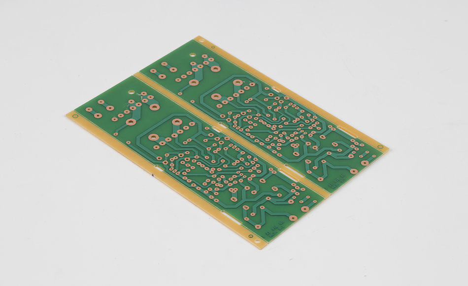
CEM3 PCB’s upgraded performance enables it to adapt to three high-growth industries, each with unique operating conditions and technical requirements. Below are its key applications and the tailored benefits it delivers.
Industrial automation systems (e.g., programmable logic controllers/PLCs, machine vision cameras, sensor nodes) operate in harsh conditions—temperature swings (-10°C to 60°C), dust, vibration, and chemical exposure. CEM3 PCB adapts to these needs by:
Resistance to Industrial Contaminants: CEM3 PCB’s epoxy matrix resists oils, coolants, and cleaning agents common in factories, preventing resin degradation that can lead to short circuits. A CEM3-based PLC used in a metalworking plant showed no signs of corrosion after 2 years of exposure to cutting fluids, while a CEM1-based PLC required replacement after 8 months.
Compatibility with Industrial Connectors: The material’s mechanical strength supports heavy-duty industrial connectors (e.g., M12 Ethernet connectors), which exert significant stress on PCBs during insertion and removal. CEM3 PCB’s reinforced edges prevent trace lifting or PCB cracking, a common issue with CEM1 PCB.
Thermal Cycling Resistance: Industrial systems often experience rapid temperature changes (e.g., from cold startup to operating temperature). CEM3 PCB withstands 1,000 thermal cycles (-40°C to 85°C) without delamination, ensuring long-term reliability.
New energy systems—such as NEV DC fast chargers and solar inverters—require substrates that can withstand outdoor conditions, high power loads, and frequent thermal cycling. CEM3 PCB meets these demands by:
High-Temperature Tolerance: CEM3 PCB’s high glass transition temperature (Tg) enables it to operate reliably in the high-heat environments of NEV chargers (where internal temperatures can reach 75°C). A CEM3-based charger module maintained stable performance for 5,000 charging cycles, while a CEM1-based module failed after 2,200 cycles due to resin softening.
Moisture and UV Resistance: For outdoor solar inverters, CEM3 PCB is formulated with UV-stabilized resin and hydrophobic additives, preventing yellowing (which reduces heat dissipation) and moisture absorption. A CEM3-based solar inverter deployed in a desert region retained 90% of its initial efficiency after 3 years, compared to 72% for a CEM1-based inverter.
Current Handling Capacity: CEM3 PCB’s thick copper traces (up to 4oz) and low resistance enable it to handle the high currents of NEV chargers (50–150A). This eliminates the need for parallel traces (common with CEM1 PCB), simplifying design and reducing failure points.
Consumer electronics—such as washing machine controllers, smart refrigerators, and home security cameras—require substrates that are affordable for mass production while reliable enough to meet 5–10 year lifespans. CEM3 PCB adapts by:
Cost-Effective Mass Production: CEM3 PCB’s compatibility with high-speed assembly lines (e.g., automated optical inspection/AOI, wave soldering) enables production of 100,000+ units/month with low labor costs. A manufacturer of smart washing machines reduced PCB production costs by 20% by switching from CEM1 to CEM3.
Resistance to Household Contaminants: CEM3 PCB’s surface resists food oils, detergents, and dust—common in household environments. A CEM3-based smart refrigerator controller showed no performance degradation after 3 years of exposure to kitchen grease, while a CEM1-based controller experienced intermittent failures due to grease buildup.
Compact Design Support: CEM3 PCB’s dimensional stability allows for dense component placement, critical for small consumer devices (e.g., smart doorbells). A CEM3-based doorbell PCB was 25% smaller than a CEM1-based version, fitting into a sleek, wall-mounted enclosure.
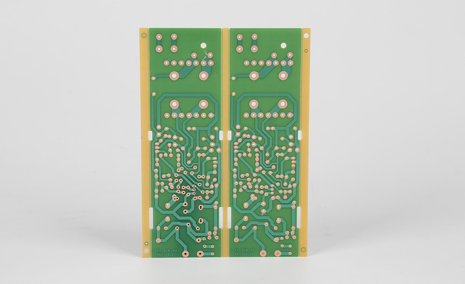
While CEM3 PCB is inherently versatile, targeted design strategies can further optimize its performance for specific industry needs. Below are actionable approaches for engineers to tailor CEM3 PCB to their applications.
Vibration-Resistant Component Mounting: Use adhesive-backed components or additional solder fillets for heavy components (e.g., industrial connectors) to distribute stress across the CEM3 PCB. A factory sensor module using this design survived 2x more vibration cycles than a module with standard mounting.
-Impedance Matching for Industrial Communication: Calculate trace widths based on CEM3’s Dk to match the impedance of industrial communication protocols (e.g., PROFINET, Modbus). This reduces signal reflections that can cause data loss. A CEM3-based PROFINET controller with impedance-matched traces achieved 99.9% data transmission accuracy, compared to 98.5% for a non-matched design.
Protective Coatings: Apply a conformal coating (e.g., polyurethane) to CEM3 PCBs in dusty or chemical-rich environments. This prevents contaminant buildup on traces, extending PCB lifespan by 3–5 years.
Thermal Via Arrays: Add thermal vias (0.3–0.5mm diameter) under high-power components (e.g., charging module MOSFETs) to transfer heat to the PCB’s bottom layer. A CEM3-based NEV charger with thermal vias reduced component temperatures by 18°C, extending lifespan by 40%.
Copper Plane Design: Use large, solid copper planes on CEM3 PCBs to spread heat from high-power components. A solar inverter using a 4oz copper plane on CEM3 reduced hot spot temperatures by 15°C compared to a 2oz plane.
UV-Resistant Solder Masks: For outdoor solar inverters, use UV-stabilized solder masks to prevent yellowing and maintain heat dissipation. A CEM3-based inverter with UV-resistant solder mask retained 95% of its heat dissipation capacity after 3 years outdoors, vs. 78% for a standard solder mask.
Double-Sided Component Placement: Use both sides of the CEM3 PCB to reduce board size. A smart doorbell PCB with double-sided components was 30% smaller than a single-sided design, fitting into a compact enclosure.
Standardized Component Footprints: Use common component footprints (e.g., 0603 resistors, SOIC-8 ICs) to avoid custom tooling costs. A smart thermostat manufacturer using standardized footprints reduced PCB design costs by 15% and shortened time-to-market by 4 weeks.
Integrated Test Points: Add test points directly to the CEM3 PCB during design, eliminating the need for separate test jigs. This reduced testing time by 25% for a washing machine controller manufacturer.
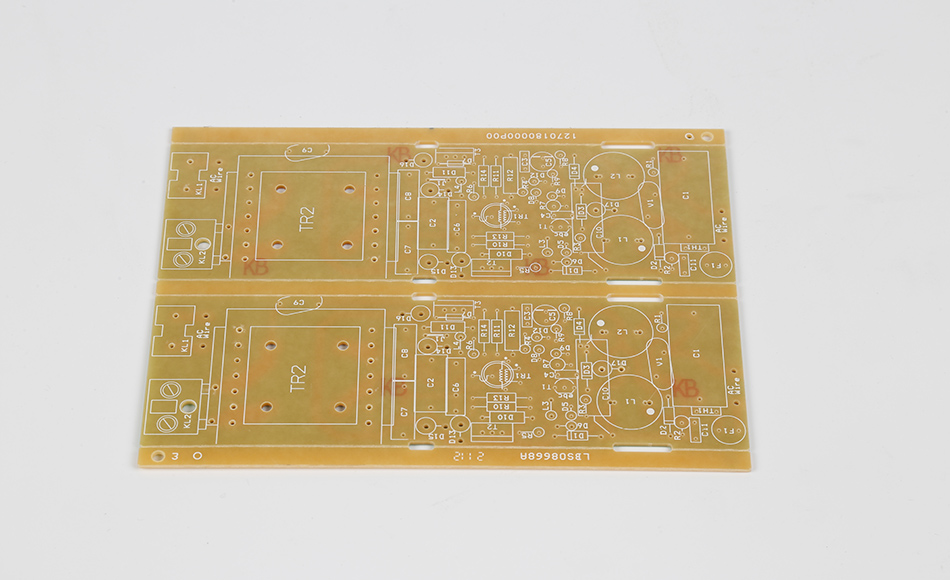
As electronic systems evolve toward greater connectivity, miniaturization, and sustainability, CEM3 PCB is adapting to meet new demands. Below are key trends shaping its future.
The growth of 5G in industrial settings (e.g., 5G-enabled machine vision, remote equipment monitoring) requires substrates with improved high-frequency performance. CEM3 PCB is evolving by:
Low-Loss Resin Formulations: New CEM3 variants use low-loss epoxy resins to reduce signal attenuation at 5G frequencies (24–39 GHz). These variants maintain signal integrity over longer traces, enabling 5G industrial gateways to operate reliably in large factories.
Controlled Impedance: Advanced manufacturing processes (e.g., laser ablation) ensure tighter impedance control (±5%) for 5G signal paths, reducing interference and data loss.
AIoT devices (e.g., edge AI sensors, smart city sensors) require small, integrated PCBs that combine sensing, processing, and communication. CEM3 PCB is adapting by:
Ultra-Thin Core Variants: 0.2–0.4mm thin-core CEM3 PCB retains mechanical strength while enabling smaller device form factors. An edge AI sensor using 0.3mm CEM3 PCB was 40% smaller than a sensor using standard 1.6mm CEM3.
Embedded Component Integration: CEM3 PCB now supports embedded passive components (e.g., resistors, capacitors), reducing component count and PCB size. An AIoT temperature sensor with embedded components had 30% fewer external parts, improving reliability and reducing assembly time.
With global focus on sustainability, CEM3 PCB is moving toward greener production:
Recycled Materials: Manufacturers are integrating recycled glass fiber (from end-of-life wind turbine blades) into CEM3 PCB, reducing carbon footprint by 20% without compromising performance.
Bio-Based Resins: Plant-derived epoxy resins (e.g., castor oil-based) are replacing petroleum-based resins in CEM3 PCB, improving biodegradability at end-of-life while retaining thermal and mechanical properties.
Energy-Efficient Production: Solar-powered curing ovens and water-based cleaning processes are reducing the energy and water usage of CEM3 PCB manufacturing by 25–30%.
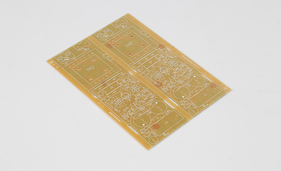
CEM3 PCB has evolved from a basic substrate to a cross-industry workhorse, driven by its upgraded mechanical resilience, stable dielectric performance, and cost-efficiency. Its ability to adapt to diverse environments—from industrial factories and new energy charging stations to household appliances—makes it a critical component in the global electronics ecosystem.
Real-world applications demonstrate its value: reduced failure rates in industrial automation, lower costs in new energy systems, and reliable performance in consumer electronics. By leveraging targeted design strategies—such as vibration-resistant mounting, thermal via arrays, and compact component placement—engineers can further unlock its potential for specific industry needs.
As electronic systems embrace 5G, AIoT, and sustainability, CEM3 PCB will continue to evolve, with upgrades in high-frequency performance, miniaturization, and eco-friendly manufacturing. For manufacturers and engineers, CEM3 PCB represents a strategic choice: it delivers the performance needed for mid-tier applications without the premium cost of specialized substrates, enabling innovation and scalability across industries.
In a market where versatility and cost control are paramount, CEM3 PCB stands as a foundational technology, supporting the next generation of reliable, efficient, and sustainable electronic systems.

Got project ready to assembly? Contact us: info@apollopcb.com


We're not around but we still want to hear from you! Leave us a note:

Leave Message to APOLLOPCB
