-
- PCB TYPE
- PRINTED CIRCUIT BOARD PROTOTYPE ALUMINUM PRINTED CIRCUIT BOARD R&F PCB FPC HIGH FREQUENCY PCB HIGH-TG PCB HEAVY COPPER PCB HDI PCB PCB FOR LIGHTING METAL CORE PCB
time:Aug 20. 2025, 16:43:56
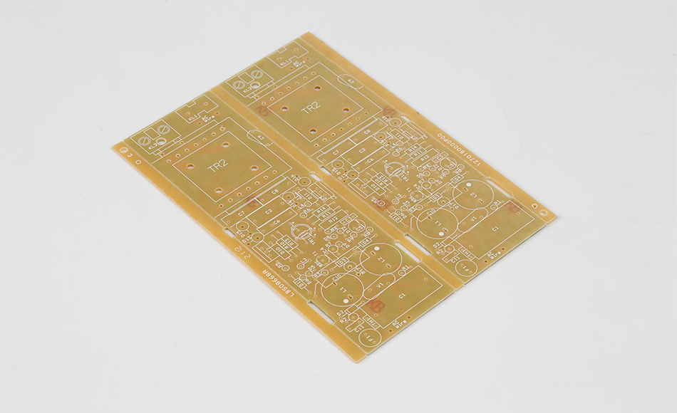
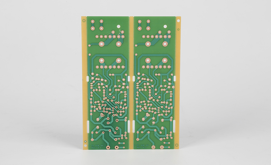
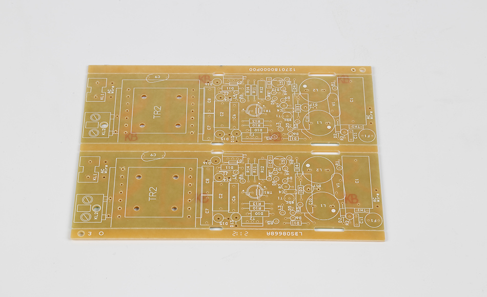
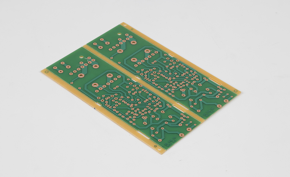
CEM3 PCB has emerged as a linchpin in the shift toward sustainable, high-performance electronics, blending cost-effectiveness with adaptability to meet the demands of modern device design. As industries grapple with stricter environmental regulations and the need for energy-efficient technologies, CEM3’s unique composition—non-woven glass core, woven glass outer layers, and epoxy resin—positions it as a versatile substrate that bridges the gap between affordability and innovation. Unlike traditional FR4, which dominates high-end applications but at a higher environmental cost, CEM3 offers a compelling balance: sufficient mechanical strength for 80% of consumer and industrial devices, coupled with a production process that reduces carbon emissions by up to 25%. This article explores CEM3 PCB’s role in sustainable manufacturing, its evolving material science, integration with emerging technologies, and its expanding footprint in sectors ranging from 5G infrastructure to green energy devices. By examining its current capabilities and future potential, we highlight how CEM3 is redefining what mid-range substrates can achieve in a rapidly changing electronics landscape.
In an era where environmental responsibility is a competitive imperative, CEM3 PCB stands out for its inherent eco-friendly attributes and ongoing advancements in green manufacturing:
CEM3’s manufacturing process consumes significantly less energy than FR4, primarily due to lower curing temperatures (150–170°C vs. 180–200°C for FR4) and simplified lamination steps. This translates to a 20–30% reduction in carbon emissions per square meter of PCB, a critical metric for brands aiming to meet net-zero targets. Additionally, CEM3’s raw material usage is more efficient: the non-woven glass core requires 15% less fiber than FR4’s fully woven structure, reducing resource extraction and waste.
Modern CEM3 PCBs increasingly use halogen-free epoxy resins, replacing brominated flame retardants with phosphorus-based alternatives that comply with EU RoHS, REACH, and California’s Proposition 65. These formulations eliminate toxic gas emissions during combustion, making end-of-life disposal safer and enabling more efficient recycling. Unlike paper-based CEM1, which degrades quickly and is difficult to recycle, CEM3’s glass fiber reinforcement allows for mechanical separation of materials, with copper recovery rates exceeding 95% and glass fibers repurposable in construction or new PCB production.
CEM3’s electrical properties—including stable dielectric constant (3.8–4.2 at 1 MHz) and low dissipation factor—contribute to energy efficiency in devices. In applications like smart home sensors or low-power IoT nodes, CEM3 minimizes signal loss, reducing the energy required for data transmission. This efficiency extends device battery life by up to 10%, aligning with consumer demand for longer-lasting, less resource-intensive electronics.

Recent advancements in CEM3’s material science have addressed historical limitations, enabling its use in previously inaccessible applications:
New CEM3 variants incorporate nano-sized aluminum oxide fillers in the epoxy matrix, improving thermal conductivity by 30% compared to traditional formulations. This allows CEM3 to dissipate heat more effectively, expanding its utility beyond low-power devices to include LED drivers, small motor controllers, and even 5G small-cell transceivers. The fillers maintain electrical insulation, ensuring safety in high-voltage scenarios up to 300V—critical for household appliances and industrial control systems.
Modified epoxy resins with higher cross-link density have boosted CEM3’s flexural strength by 20%, making it suitable for ruggedized applications like portable industrial scanners and outdoor IoT sensors. These resins also enhance adhesion between glass fibers and copper cladding, reducing delamination risks in humid environments (e.g., bathroom electronics or agricultural monitors). In bend tests, modern CEM3 PCBs withstood 5,000+ cycles at a 15mm radius without cracking, outperforming older versions by 2x.
Through resin chemistry tweaks—including the addition of silica nanoparticles—CEM3 now maintains stable dielectric properties up to 2 GHz, a range previously dominated by FR4. This makes it viable for 5G indoor routers, Wi-Fi 6E access points, and smart meters, where signal integrity at high frequencies is critical. The nanoparticles reduce signal loss by minimizing moisture absorption, ensuring consistent performance in varying environmental conditions.

CEM3’s adaptability has made it a cornerstone of several fast-growing tech sectors, where its balance of performance and cost drives innovation:
While 5G macro base stations rely on FR4 for high-power handling, CEM3 PCBs are widely used in small cells, indoor distributed antenna systems (DAS), and IoT gateways. Their ability to support 2 GHz frequencies, combined with lower weight (15% lighter than FR4), makes them ideal for mounting on walls or ceilings. In urban deployments, CEM3-based small cells reduce installation costs by 25% while meeting signal quality requirements for dense urban networks.
CEM3 PCBs play a key role in renewable energy systems, including solar micro-inverters, wind turbine sensors, and battery management systems (BMS). Their halogen-free formulations align with green energy standards, while improved thermal conductivity ensures reliable operation in high-temperature environments (e.g., solar panel enclosures). In BMS for electric vehicles (EVs), CEM3’s mechanical stability protects against vibration, ensuring accurate monitoring of battery health.
Edge computing nodes—deployed in factories, retail stores, or smart cities—require compact, energy-efficient PCBs, and CEM3 fits the bill. Its support for high-density components (e.g., 0.8mm pitch ICs) and compatibility with surface-mount technology (SMT) enables the miniaturization needed for edge devices. In smart retail systems, CEM3-based PCBs power inventory scanners and digital shelf labels, with low power consumption extending battery life to 5+ years.
The healthcare sector leverages CEM3’s biocompatible variants (with medical-grade epoxy resins) in wearable monitors, such as continuous glucose trackers and ECG patches. These PCBs offer the necessary flexibility for skin contact, while their durability withstands daily wear and exposure to sweat. CEM3’s cost-effectiveness also enables mass production of disposable medical sensors, reducing healthcare costs without compromising reliability.

CEM3 PCB’s compatibility with cutting-edge manufacturing processes has accelerated its adoption, enabling higher precision and scalability:
CEM3’s dimensional stability—even during reflow soldering (up to 260°C)—makes it ideal for automated SMT lines. Unlike flexible PCBs, which require specialized handling, CEM3 can be processed on standard assembly equipment, reducing factory retooling costs. In high-volume production (e.g., smartphone chargers or smart bulbs), CEM3’s consistent material properties lower defect rates to under 0.5%, outperforming paper-based substrates by 3x.
Emerging 3D printing techniques for electronics—such as inkjet deposition of conductive traces—work seamlessly with CEM3 substrates. The material’s porous non-woven core allows for better adhesion of printed inks, enabling rapid prototyping of custom PCBs for niche applications (e.g., industrial sensors or medical devices). This compatibility reduces lead times from weeks to days, accelerating product development cycles.
Machine vision systems, paired with AI algorithms, now inspect CEM3 PCBs for defects like fiber fraying or resin unevenness with 99.9% accuracy. These systems learn from material variations across batches, adjusting inspection parameters to account for CEM3’s inherent slight inconsistencies. This ensures that only high-quality boards proceed to assembly, reducing waste and improving overall yield.

CEM3 PCB’s unique positioning becomes clear when compared to other substrates across critical metrics:
FR4 offers superior thermal and mechanical performance but at a 40–60% higher cost and 25% higher carbon footprint. For applications like smart TVs or home routers—where operating temperatures stay below 85°C and vibration is minimal—CEM3 delivers equivalent reliability at a fraction of the environmental cost. Only in high-power devices (e.g., EV chargers) or extreme environments (e.g., aerospace) does FR4’s premium justify its use.
FPCs excel in curved designs (e.g., smartwatch bands) but cost 3–5x more than CEM3. For flatter wearables—such as fitness bands or medical patches—thinned CEM3 (0.6mm) offers sufficient flexibility at 1/4 the price. Its rigidity also simplifies component mounting, reducing assembly complexity in high-volume production.
MCPCBs dissipate heat better in high-power LEDs (e.g., stadium lights), but CEM3 is preferable for low-to-moderate power applications (e.g., residential LED bulbs). CEM3’s lower thermal conductivity (0.3–0.5 W/mK vs. 2–5 W/mK for MCPCB) is sufficient for 10–50W bulbs, while its lighter weight and lower cost reduce shipping emissions and consumer prices.

Ongoing research and development promise to further expand CEM3’s capabilities, solidifying its role in future technologies:
Scientists are developing CEM3 variants using epoxy resins derived from renewable sources, such as soybean oil or lignin. These bio-resins reduce reliance on petroleum by 50% and lower carbon emissions by an additional 15%. Early tests show they maintain mechanical strength, with potential applications in consumer electronics and packaging.
With 6G trials targeting 100+ GHz frequencies, CEM3 is being engineered to maintain dielectric stability at these bands. New resin formulations with fluorinated additives aim to reduce signal loss, potentially making CEM3 a cost-effective option for 6G small cells and IoT devices requiring ultra-fast data transfer.
CEM3’s porous structure makes it suitable for integrating energy-harvesting materials, such as piezoelectric films or thermoelectric generators. Researchers are testing CEM3-based PCBs that capture ambient vibration or heat, powering low-energy devices like smart sensors without batteries. This could eliminate e-waste from disposable batteries, aligning with circular economy goals.
CEM3 PCB has evolved from a budget-friendly alternative to a sustainable, high-performance substrate driving innovation across electronics. Its ability to balance environmental responsibility, mechanical resilience, and cost-effectiveness makes it indispensable in 5G infrastructure, green energy devices, and medical wearables, among other sectors. As material science advances—from bio-based resins to high-frequency compatibility—CEM3 is poised to capture new markets, challenging the dominance of more expensive substrates in applications where “good enough” is being redefined as “excellent.” For manufacturers, engineers, and brands, CEM3 represents a strategic choice: a substrate that meets today’s sustainability demands while enabling tomorrow’s technological breakthroughs. In a world where electronics must be both powerful and planet-friendly, CEM3 PCB is leading the way.

Got project ready to assembly? Contact us: info@apollopcb.com


We're not around but we still want to hear from you! Leave us a note:

Leave Message to APOLLOPCB
