-
- PCB TYPE
- PRINTED CIRCUIT BOARD PROTOTYPE ALUMINUM PRINTED CIRCUIT BOARD R&F PCB FPC HIGH FREQUENCY PCB HIGH-TG PCB HEAVY COPPER PCB HDI PCB PCB FOR LIGHTING METAL CORE PCB
time:Dec 16. 2025, 11:53:45
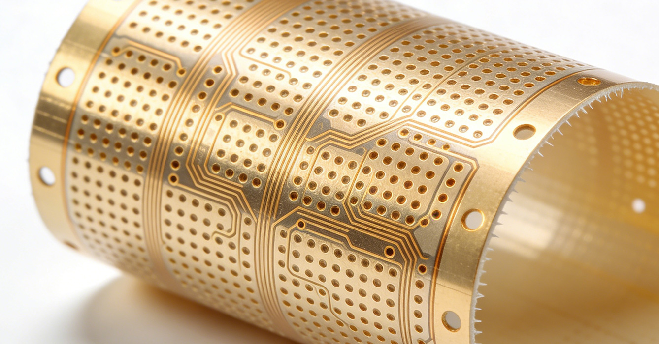
As electronic devices pursue extreme miniaturization, high functionality, and reliable flexibility, HDI Blind/Buried Vias Flexible PCB has emerged as a critical enabling technology. By integrating high-density interconnect (HDI) design with blind and buried via structures on flexible substrates, this specialized circuit solution breaks through the spatial limitations of traditional flexible PCBs, achieving denser line layout and more efficient layer-to-layer interconnection. Unlike standard flexible PCBs that rely on through-holes, HDI Blind/Buried Vias Flexible PCB minimizes substrate damage, optimizes signal transmission, and supports the compact design of high-end electronic products. For industries such as foldable electronics, automotive intelligence, and precision medical devices, this technology has become a key driver of product innovation and performance upgrading.
The unique structural design of HDI Blind/Buried Vias Flexible PCB endows it with unparalleled advantages in high-density integration and reliable operation, addressing core pain points of traditional flexible circuits:
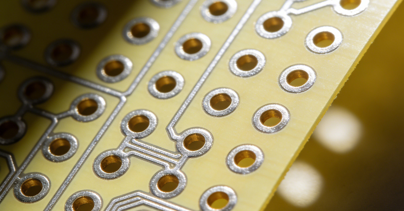
- Enhanced Spatial Utilization & Miniaturization: Blind vias (connecting surface layers to specific inner layers) and buried vias (connecting inner layers without penetrating the surface) eliminate the space occupation of through-holes that penetrate the entire substrate. This allows more circuits and components to be arranged on limited flexible substrates, significantly reducing the overall size of the PCB while reserving more installation space for other precision components. This advantage is particularly critical for ultra-thin devices such as foldable smartphones and AR/VR headsets.
- Optimized Signal Integrity & High-Frequency Performance: Traditional through-holes lengthen signal transmission paths and easily cause inter-layer crosstalk. HDI blind/buried vias shorten signal transmission distances, reducing signal attenuation and delay. Additionally, the non-penetrating structure reduces external electromagnetic interference and internal signal radiation, ensuring stable signal transmission even in high-frequency scenarios such as 5G communication modules and automotive millimeter-wave radar systems.
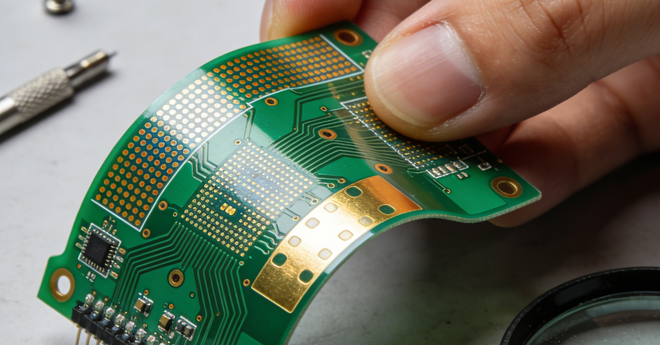
- Improved Flexibility & Durability: The absence of through-holes reduces stress concentration points on the flexible substrate during bending. This enhances the board's flex fatigue resistance, extending its service life in applications requiring frequent bending, such as foldable screen hinges and wearable device straps. The flat surface without through-hole protrusions also improves the fit with other components, reducing assembly damage risks.

The production of HDI Blind/Buried Vias Flexible PCB requires precise control across the entire process, with key breakthroughs addressing the unique challenges of combining HDI technology with flexible substrates:
- Precision Positioning for Blind/Buried Vias: Flexible substrates are prone to deformation under temperature and mechanical stress, making accurate via positioning a major challenge. Advanced laser drilling technology with micron-level precision is adopted to achieve precise alignment of blind/buried vias, ensuring reliable interconnection between target layers. Real-time visual positioning systems monitor the drilling process, compensating for substrate deformation in real time to avoid alignment errors.
- Reliable Via Wall Quality & Plating: Via wall roughness, burrs, and insufficient plating adhesion are common issues in blind/buried via processing. Specialized drilling tools and process parameters are used to minimize via wall damage, while high-performance plating solutions with excellent throwing power ensure uniform and dense copper plating on via walls. Nitrogen protection during the drilling and plating processes prevents oxidation, enhancing the electrical conductivity and mechanical strength of the vias.
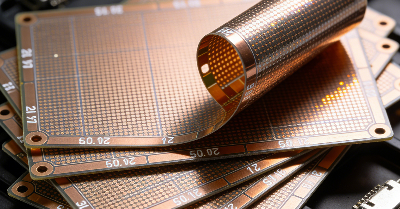
- Controlled Multilayer Lamination & Stress Management: Multilayer HDI Blind/Buried Vias Flexible PCB requires precise lamination of multiple flexible layers. Temperature and pressure-controlled lamination processes are employed to ensure tight bonding between layers without resin overflow or voids. Post-lamination stress relief treatments reduce internal stress caused by thermal expansion differences, preventing substrate warpage and ensuring dimensional stability.

HDI Blind/Buried Vias Flexible PCB has become a preferred solution in key high-end application fields, enabling technological innovation through its unique performance advantages:
- Foldable & Wearable Electronics: In foldable smartphones and tablets, it is used in hinge modules and flexible display connections, supporting hundreds of thousands of bending cycles while maintaining stable signal transmission. For wearable health monitors, its miniaturized and high-density design integrates sensor circuits, power management, and wireless communication modules into a small, flexible form factor.
- Automotive Intelligent Systems: It is widely used in automotive millimeter-wave radar, lidar, and smart cockpit systems. The high signal integrity ensures accurate data transmission for autonomous driving sensors, while its resistance to vibration and extreme temperatures meets the strict reliability requirements of automotive electronics. The compact design also helps reduce the weight of automotive electronic systems.
- Precision Medical Devices: In miniaturized medical devices such as implantable pacemakers and minimally invasive surgical instruments, HDI Blind/Buried Vias Flexible PCB enables high integration of functional circuits in limited space. Its biocompatible substrate options and reliable performance ensure safe and stable operation in the human body environment.

The development of HDI Blind/Buried Vias Flexible PCB is focusing on higher integration, better reliability, and more eco-friendly manufacturing to meet evolving market demands:
- Ultra-High-Density Integration: Ongoing advancements in laser drilling and circuit etching technologies will enable even smaller via sizes and finer line widths, further improving integration density to support the development of more complex and miniaturized electronic devices.
- Material & Process Synergy: Integration of high-performance substrates such as liquid crystal polymer (LCP) with advanced blind/buried via processes will enhance high-frequency performance and thermal stability, expanding applications in 6G communication and high-power electronic systems.
- Intelligent Quality Control: Adoption of AI-driven automated inspection systems will enable real-time detection of via defects, layer alignment issues, and circuit faults, improving production yield and reducing manufacturing costs.

In conclusion, HDI Blind/Buried Vias Flexible PCB represents a major advancement in flexible circuit technology, addressing the critical need for high-density integration in next-generation electronics. Through its unique technical advantages, refined manufacturing processes, and targeted high-end applications, it is driving innovation across multiple industries. As electronic devices continue to evolve toward miniaturization and intelligence, the strategic importance of HDI Blind/Buried Vias Flexible PCB will continue to grow, becoming a core component in shaping the future of electronic manufacturing.

Got project ready to assembly? Contact us: info@apollopcb.com


We're not around but we still want to hear from you! Leave us a note:

Leave Message to APOLLOPCB
