-
- PCB TYPE
- PRINTED CIRCUIT BOARD PROTOTYPE ALUMINUM PRINTED CIRCUIT BOARD R&F PCB FPC HIGH FREQUENCY PCB HIGH-TG PCB HEAVY COPPER PCB HDI PCB PCB FOR LIGHTING METAL CORE PCB
time:Oct 29. 2025, 13:07:48
Printed Circuit Boards (PCBs) are the backbone of most electronic devices, from simple gadgets to complex machinery. Understanding the PCB assembly process is essential for anyone involved in electronics manufacturing or design. This article will guide you through each stage of the process, explaining key concepts and terms along the way.
PCB assembly refers to the process of attaching various electronic components to a PCB to create a functional circuit board. This process is crucial in electronics manufacturing, as it transforms a blank circuit board into a working product.

Before assembly can begin, a PCB design must be created. This involves using specialized software to layout the circuit, placing components, and routing electrical connections. The design process must also consider the physical constraints of the product, such as size and shape.
Once the design is finalized, the PCB is manufactured. This involves several steps:
Substrate Preparation: The substrate, usually made of fiberglass or plastic, is coated with a layer of copper.
Etching: A chemical process removes unwanted copper, leaving only the desired circuit pattern.
Drilling: Holes are drilled in the board to accommodate component leads and vias.
Plating: The holes are plated with copper to ensure electrical conductivity.
Solder paste is applied to the board's surface to prepare it for component placement. This paste consists of tiny solder balls suspended in a flux, which helps the solder adhere to the board during reflow.
During this step, components are placed onto the board. This can be done manually or using automated machines known as pick-and-place machines. The machine uses the PCB design files to accurately place each component in its designated spot.
There are two main types of soldering used in PCB assembly:
Reflow Soldering: This method is used for surface-mount technology (SMT) components. The board is heated in a reflow oven, causing the solder paste to melt and form a solid connection.
Wave Soldering: This is used for through-hole components. The board passes over a wave of molten solder, which adheres to exposed metal areas.
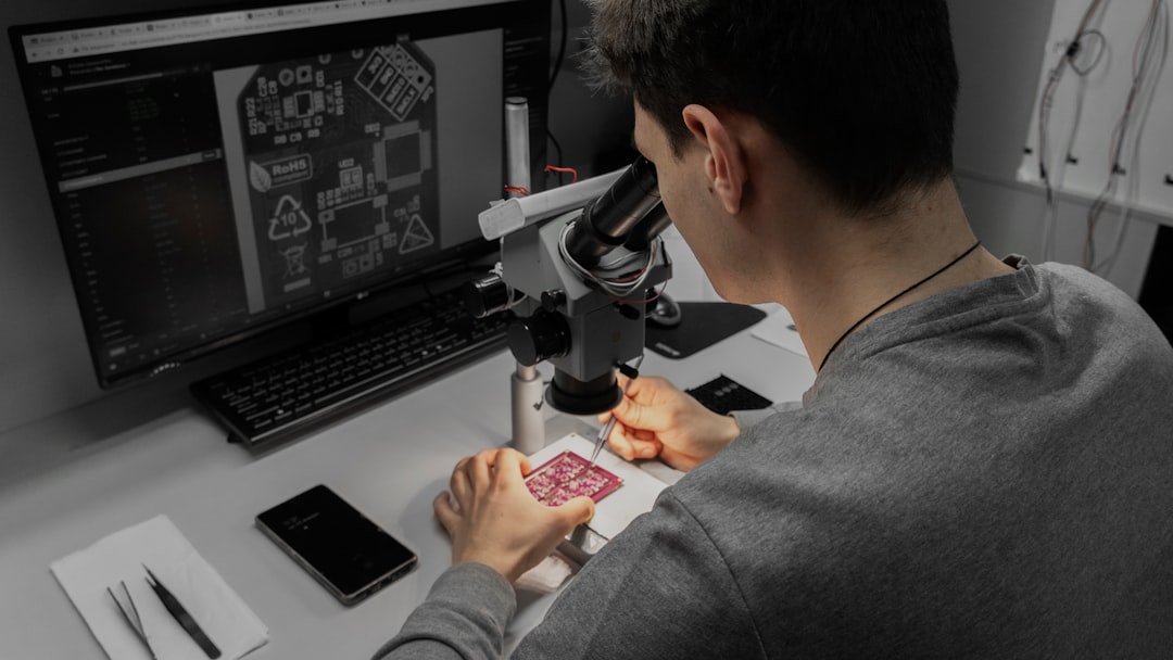
Once the board is assembled, it undergoes rigorous inspection and testing to ensure functionality. This can involve visual inspections, automated optical inspections (AOI), and electrical testing. These steps are crucial to catch any defects or errors before the boards move on to final assembly.

While PCB assembly is a well-established process, it presents several challenges:
Component Sourcing: Finding the right components at the right price can be difficult, especially during shortages.
Design Complexity: As devices become more advanced, PCB designs become more complex, increasing the risk of errors.
Quality Control: Ensuring every board meets quality standards requires thorough testing and inspection.
Effective PCB assembly requires collaboration between designers, manufacturers, and assemblers. Clear communication ensures that everyone understands the requirements and constraints of the project, reducing the risk of errors and delays.
Choosing the right PCB manufacturer is crucial for successful assembly. Consider the following when selecting a partner:
Experience: Look for manufacturers with a proven track record in PCB assembly.
Capabilities: Ensure the manufacturer can handle the complexity and volume of your project.
Quality Assurance: A strong quality assurance program is essential to produce reliable boards.

The PCB assembly process continues to evolve, driven by technological advancements and industry demands. Some notable innovations include:
Flexible PCBs: These boards can bend and twist, allowing for more versatile designs.
Advanced Materials: New materials, such as high-temperature laminates, enable boards to withstand extreme conditions.
Automation: Increased automation in assembly processes improves accuracy and efficiency.
Understanding the PCB assembly process is essential for anyone involved in electronics design or manufacturing. By grasping the steps involved and the challenges faced, you can make informed decisions and collaborate effectively with partners. As technology advances, staying updated on the latest trends and innovations will ensure your projects remain competitive and successful.
With this comprehensive guide, you are now better equipped to navigate the intricate world of PCB assembly. Whether you're designing a simple gadget or a complex system, understanding these fundamentals will help you achieve your goals.

Got project ready to assembly? Contact us: info@apollopcb.com


We're not around but we still want to hear from you! Leave us a note:

Leave Message to APOLLOPCB
