-
- PCB TYPE
- PRINTED CIRCUIT BOARD PROTOTYPE ALUMINUM PRINTED CIRCUIT BOARD R&F PCB FPC HIGH FREQUENCY PCB HIGH-TG PCB HEAVY COPPER PCB HDI PCB PCB FOR LIGHTING METAL CORE PCB
time:Nov 10. 2025, 15:32:51
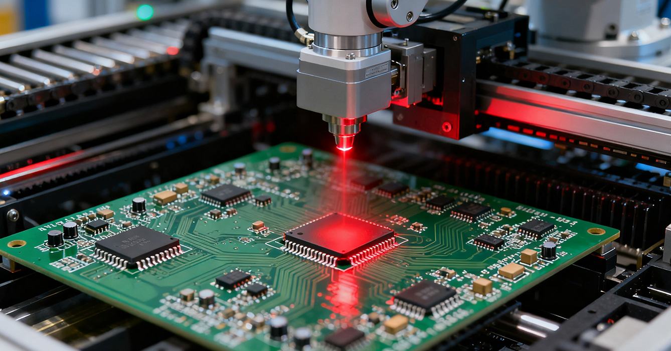
PCB Assembly is no longer a linear post-design process but a collaborative ecosystem where design and production teams work in lockstep to accelerate innovation and cut time-to-market. In today’s fast-paced electronics industry, delays caused by poor design-manufacturing alignment—such as unproducible layouts or last-minute component substitutions—can cost businesses millions in lost market share. The new paradigm of design-production synergy integrates PCB design decisions with assembly feasibility from day one, leveraging digital tools, cross-functional communication, and iterative feedback to create a seamless workflow. This approach not only reduces rework and production bottlenecks but also ensures assemblies are optimized for both performance and manufacturability. This article explores how design-production synergy redefines PCB assembly, its key enablers, industry-specific outcomes, and its impact on competitive advantage.

Effective synergy relies on three interconnected strategies that bridge the gap between design and manufacturing:
- Early-Stage DFM Integration: Design for Manufacturability (DFM) reviews are no longer a final check but an ongoing process starting in the schematic design phase. Assembly engineers collaborate with designers to flag issues like overly tight trace spacing, incompatible component footprints, or high-cost materials. For example, a designer might adjust a BGA placement to avoid solder shadowing after an assembly team highlights potential reflow challenges—eliminating a costly redesign later.
- Real-Time Production Feedback Loops: During prototype assembly, production teams share data on defect rates, solder paste performance, and component availability with designers in real time. If a prototype has consistent tombstoning of 0201 resistors, the design team can modify pad sizes or component orientation while the production line adjusts placement parameters—resolving the issue in hours instead of weeks.
- Digital Twin Collaboration: Virtual replicas of both the PCB design and assembly line let teams simulate production before physical manufacturing. Designers can test how changes to component placement affect pick-and-place efficiency, while assembly teams can validate stencil designs or reflow profiles in a digital environment. This simulation reduces the need for physical prototypes by 40–50% and cuts NPI (New Product Introduction) time by up to 30%.

Cloud-based design-manufacturing platforms (e.g., Altium 365, Siemens Xcelerator) let designers and assembly teams access shared Gerber files, BOMs, and test data in real time. These platforms include built-in DFM checkers that auto-generate assembly feasibility reports, flagging issues like non-standard components or suboptimal aperture designs.
Training programs teach designers basic assembly principles (e.g., solder paste volume requirements, component sourcing challenges) and assembly teams design fundamentals (e.g., signal integrity, thermal management). This shared knowledge reduces communication gaps—an assembly technician, for instance, might recognize that a designer’s choice of a heat-sensitive component conflicts with reflow temperatures and suggest a compatible alternative.

Smartphone manufacturers use synergy to launch new models annually. By integrating design and assembly teams, they optimize PCB layouts for high-volume SMT lines—e.g., standardizing component sizes to reduce changeover time between production runs. This collaboration has cut NPI time for flagship phones from 12 to 8 months, enabling brands to respond faster to consumer trends like foldable displays.
Industrial PCB assemblies require both ruggedness and precision. Synergy ensures designs balance thermal management (for factory environments) with manufacturability—e.g., a design team might use larger thermal vias after assembly tests show overheating in prototype units. This reduces field failures by 25% and extends product lifespan.
Regulatory compliance adds complexity to medical PCB assembly. Synergy lets design and assembly teams align on standards like ISO 13485 early—e.g., ensuring traceable components are specified in the BOM and cleanroom-compatible layouts are used. This streamlines regulatory approval by 30%, getting life-saving devices to market faster.

Advancements in AI and connectivity will deepen collaboration further:
- AI-Powered Design Assistants: Machine learning tools will suggest assembly-optimized design changes (e.g., component substitutions for better availability) in real time, based on production data.
- Edge-to-Cloud Data Integration: IoT sensors on assembly lines will feed real-time production data into design platforms, letting AI adjust designs dynamically for shifting conditions (e.g., component shortages).
PCB Assembly’s future lies in design-production synergy—not as separate functions but as a unified ecosystem. By integrating DFM early, creating real-time feedback loops, and leveraging digital twins, businesses can cut time-to-market, reduce costs, and deliver higher-quality assemblies. In an industry where speed and innovation are paramount, this collaborative approach is no longer a luxury but a necessity. For manufacturers, investing in design-production synergy means not just building better PCBs, but building them faster and more efficiently—gaining a critical edge in the race to meet consumer and industry demands.

Got project ready to assembly? Contact us: info@apollopcb.com


We're not around but we still want to hear from you! Leave us a note:

Leave Message to APOLLOPCB
