-
- PCB TYPE
- PRINTED CIRCUIT BOARD PROTOTYPE ALUMINUM PRINTED CIRCUIT BOARD R&F PCB FPC HIGH FREQUENCY PCB HIGH-TG PCB HEAVY COPPER PCB HDI PCB PCB FOR LIGHTING METAL CORE PCB
time:Nov 12. 2025, 11:04:07
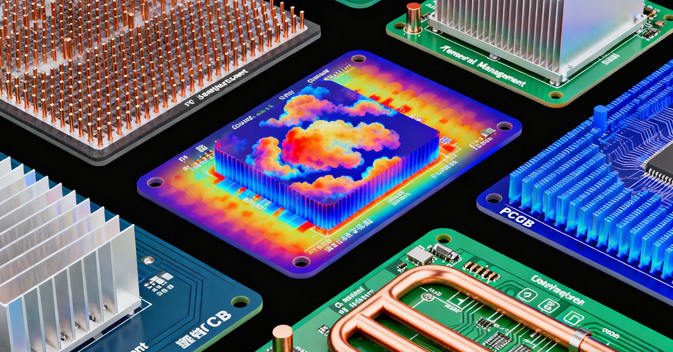
PCB Thermal Management is the backbone of electronic device reliability, encompassing a suite of design, material, and operational practices that control heat generation, transfer, and dissipation throughout a PCB’s lifecycle. Unlike specialized thermal solutions (e.g., active cooling or direct thermal paths) that target specific challenges, foundational PCB thermal management focuses on proactive, cross-functional optimization—aligning PCB layout, component selection, and environmental adaptation to prevent heat-related failures across consumer, industrial, and medical electronics. As devices shrink in size while handling higher power (e.g., wearable health monitors, outdoor IoT sensors, and industrial control units), effective thermal management moves beyond "fixing hotspots" to building heat resilience into every design decision. This article explores the core foundational strategies, material-geometry synergy, application-specific adaptations, and lifecycle-focused practices that define robust PCB thermal management.
These strategies form the basis of heat-resilient PCB design, applicable across most electronic systems:
Component layout is the first line of defense against heat buildup, with two key principles:
Heat Source Segregation: High-power components (e.g., voltage regulators, RF modules) are placed away from heat-sensitive parts (e.g., microcontrollers, sensors) to avoid thermal crosstalk. For example, in a smart thermostat PCB, the power supply module is positioned at the edge—far from the temperature sensor that drives control logic.
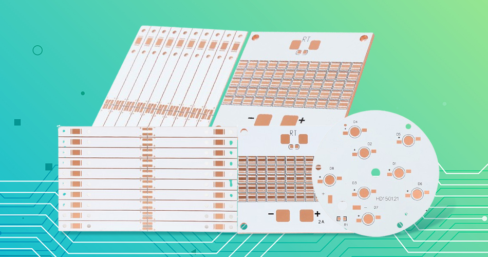
Uniform Heat Distribution: Components with similar heat outputs are spaced evenly to prevent concentrated hotspots. In a LED strip PCB, LEDs are arranged in a grid with equal spacing, ensuring no single area bears excessive thermal load.
Copper layers act as the primary thermal "highways" in PCBs, and strategic layout enhances heat spread:
Thermal Pour Design: Solid copper pours (connected to ground or power planes) are placed beneath high-power components to absorb and distribute heat. Pour boundaries are shaped to avoid blocking signal traces, balancing thermal performance and electrical functionality.
Thermal Via Placement: Vias (plated through-holes) connect top-layer heat sources to inner or bottom copper planes, creating vertical heat paths. Unlike dense via arrays for extreme power, foundational designs use "staggered" vias—spaced to maximize heat transfer without compromising PCB structural integrity.
Passive solutions remain critical for low-to-medium power devices, integrated early in design:
Heat Sink Compatibility: PCB pads for high-power components are sized to match standard low-profile heat sinks, eliminating the need for custom adapters. For example, a power transistor pad is designed to fit a 10mm x 10mm heat sink, ensuring easy assembly and effective heat transfer.
Chassis Thermal Coupling: PCB edges or dedicated mounting points are designed to connect to the device chassis, using the chassis as a secondary heat sink. This is common in consumer electronics (e.g., laptop motherboards) where the device’s metal frame acts as a passive cooler.

The combination of PCB materials and physical geometry directly impacts heat handling:
Standard FR-4 Enhancements: For low-power devices (e.g., smartwatches), thermally enhanced FR-4 (with ceramic fillers) replaces standard FR-4, boosting thermal conductivity by 30–40% without increasing cost.
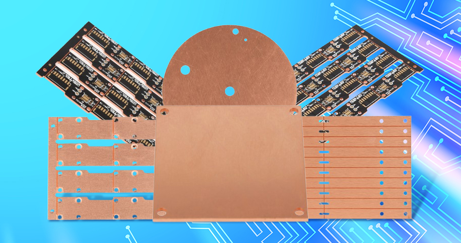
Specialized Substrates for High Loads: For industrial PCBs (e.g., motor controllers), metal-core PCBs (MCPCBs) or ceramic substrates are used. MCPCBs, with an aluminum core, conduct heat 5–10x faster than FR-4, ideal for sustained high-power operation.
Layer Count Alignment: More copper layers (e.g., 6-layer vs. 4-layer PCBs) provide additional thermal paths, but layer count is matched to power needs. A 2-layer PCB suffices for a low-power sensor, while a 6-layer PCB is used for a mid-power industrial router.
Thickness Balance: Thicker PCBs (e.g., 1.6mm vs. 1.0mm) offer better heat retention, but thickness is optimized for device enclosure constraints. A wearable PCB uses a 0.8mm thin design with reinforced copper layers to balance heat management and flexibility.

Foundational strategies are tailored to unique environmental and functional demands:
Wearables (e.g., fitness trackers) require thermal management that avoids skin discomfort:
Flexible Thermal Paths: Copper-polyimide composites form flexible heat paths that bend with the device, directing heat to less skin-contacting areas (e.g., the device’s edge instead of the back).
Low-Profile Design: No external heat sinks—heat is dissipated via the PCB’s top layer and the device’s plastic enclosure, which is textured to increase surface area for passive cooling.
Sensors in harsh environments (e.g., agricultural weather stations) need thermal resilience against temperature swings:
Thermal Insulation Layers: A thin layer of heat-resistant material (e.g., silicone) is added between the PCB and enclosure, preventing extreme ambient temperatures (e.g., -30°C to 60°C) from affecting components.
Solar Load Mitigation: PCB layout avoids dark-colored components or copper areas in direct sunlight, reducing solar heat absorption.
Implantable or diagnostic devices (e.g., glucose monitors) require low-heat, biocompatible designs:
Low-Power Component Selection: Thermal management starts with choosing low-heat components (e.g., ultra-low-power microcontrollers), minimizing heat generation at the source.
Biocompatible Thermal Coatings: PCBs are coated with biocompatible materials (e.g., parylene) that insulate components while allowing gentle heat dissipation to body tissue.

Robust PCB thermal management extends beyond design to operation and maintenance:
Thermal Testing During Prototyping: Early prototypes undergo thermal cycling (e.g., -20°C to 85°C) to simulate real-world use, identifying heat-related weaknesses before mass production.
Field Monitoring for Industrial PCBs: Industrial PCBs include embedded temperature sensors that send data to a central system, alerting operators to abnormal heat levels (e.g., due to dust buildup) that require maintenance.
PCB Thermal Management is not a one-time technical task but a holistic practice that integrates design, materials, and application needs. By focusing on foundational strategies—thermal-aware placement, copper optimization, and passive cooling—engineers build PCBs that withstand heat challenges across diverse ecosystems, from wearables to industrial control systems. As electronics continue to miniaturize and diversify, these foundational practices remain essential, ensuring reliability without overcomplicating designs or inflating costs. For manufacturers, prioritizing these basics ensures that thermal management supports, rather than limits, device innovation and performance.

Got project ready to assembly? Contact us: info@apollopcb.com


We're not around but we still want to hear from you! Leave us a note:

Leave Message to APOLLOPCB
