-
- PCB TYPE
- PRINTED CIRCUIT BOARD PROTOTYPE ALUMINUM PRINTED CIRCUIT BOARD R&F PCB FPC HIGH FREQUENCY PCB HIGH-TG PCB HEAVY COPPER PCB HDI PCB PCB FOR LIGHTING METAL CORE PCB
time:Oct 24. 2025, 18:11:08
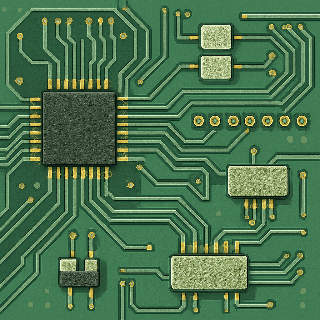
Printed Circuit Boards (PCBs) are the backbone of most electronic devices we use today. From the smartphone in your pocket to the computer on your desk, PCBs are an essential component. But how do these intricate boards come to life? Let's delve into the PCB assembly process to understand how they are designed and manufactured.
PCB assembly is the process of connecting electronic components to the printed circuit board to create a fully functional electronic device. It involves several steps, from designing the PCB layout to soldering components onto the board. This process is crucial for the performance and reliability of the final electronic product.

Understanding the steps involved in PCB assembly can help you appreciate the complexity and precision required in creating electronic devices.
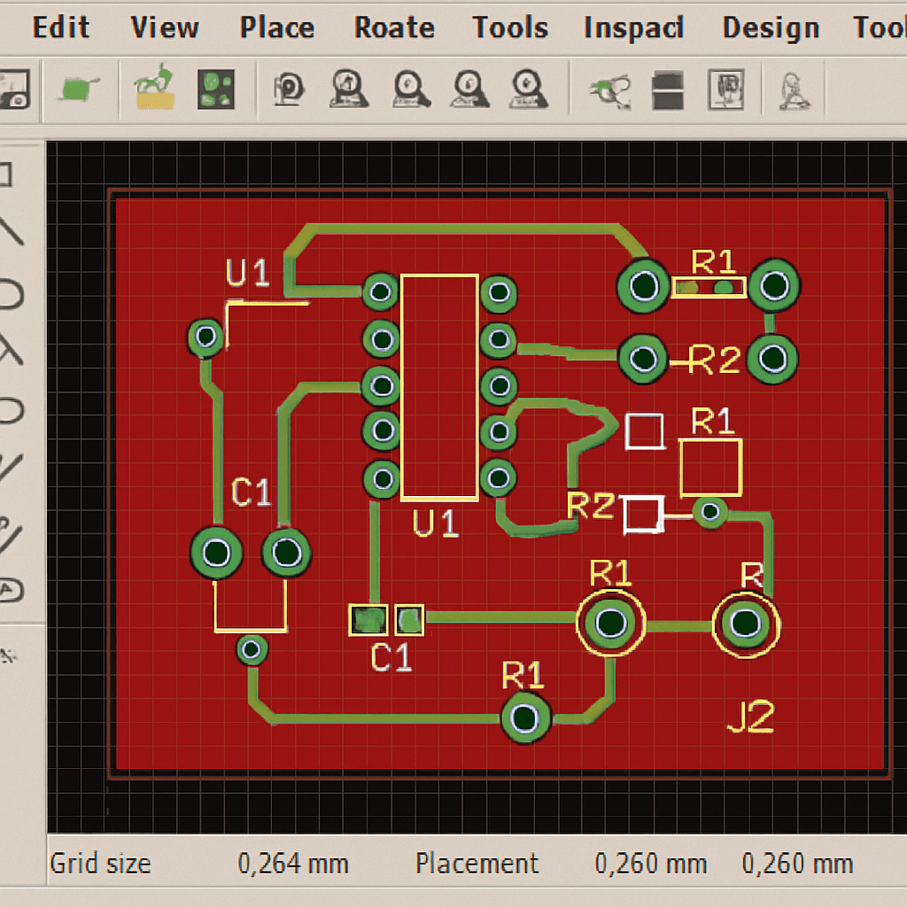
The first step in the PCB assembly process is designing the layout. Engineers use specialized software to map out where each component will be placed on the board. This design phase is critical as it determines how efficiently the board will function.
Once the design is complete, the next step is to print the PCB. This involves transferring the design onto a physical board. The board is typically made from a non-conductive material, like fiberglass, and coated with a copper layer. The design is etched onto the board, creating paths for electricity to flow between components.
Solder paste is applied to the board where components will be placed. This paste is a mixture of tiny solder balls and flux, which helps the solder adhere to the board. The paste is applied using a stencil that matches the design of the board.
After the solder paste is applied, the next step is to place the components onto the board. This is usually done using a pick-and-place machine that accurately positions each component onto the board. This step requires precision to ensure that each component aligns perfectly with the solder paste.
Once all components are placed, the board undergoes a soldering process. There are two main types of soldering used in PCB assembly: reflow soldering and wave soldering.
Reflow Soldering: This is the most common method for surface-mounted components. The board is passed through a reflow oven, where the solder paste melts and forms a solid connection between the board and components.
Wave Soldering: Used mainly for through-hole components, this method involves passing the board over a wave of molten solder. This process ensures that the solder reaches the underside of the board and secures the components in place.
After soldering, the PCB undergoes a thorough inspection and testing process. This step is crucial to ensure that the board functions as intended. Inspections can be done visually or using automated optical inspection (AOI) systems that check for defects like misaligned components or soldering issues.
The final step in the PCB assembly process is assembling the board into its final housing. This involves attaching any additional components, such as connectors or cables, and securing the board into its enclosure.

The PCB assembly process is not without its challenges. Here are some common issues that engineers face:
Design Flaws: Errors in the design phase can lead to costly mistakes later in the assembly process. It's crucial to thoroughly review and test the design before proceeding to manufacturing.
Component Availability: Sometimes, the components specified in the design may not be readily available, leading to delays in the assembly process.
Soldering Defects: Issues like solder bridges or cold joints can affect the performance of the board. Careful inspection and testing are necessary to catch these defects early.
PCB assembly is a vital step in the production of any electronic device. It ensures that all components are correctly connected and that the device will function as intended. The precision and quality of the assembly process directly impact the performance and reliability of the final product.

The PCB assembly process is a complex but fascinating journey from design to a fully functional electronic device. By understanding each step, from PCB design to final assembly, we gain a deeper appreciation for the technology that powers our modern world. Whether you're an engineer, a hobbyist, or simply curious about electronics, understanding PCB assembly is key to grasping the intricacies of electronic manufacturing.
With this knowledge, you're better equipped to tackle any challenges that arise in PCB design and manufacturing, ensuring the creation of reliable and efficient electronic products.

Got project ready to assembly? Contact us: info@apollopcb.com


We're not around but we still want to hear from you! Leave us a note:

Leave Message to APOLLOPCB
