-
- PCB TYPE
- PRINTED CIRCUIT BOARD PROTOTYPE ALUMINUM PRINTED CIRCUIT BOARD R&F PCB FPC HIGH FREQUENCY PCB HIGH-TG PCB HEAVY COPPER PCB HDI PCB PCB FOR LIGHTING METAL CORE PCB
time:Oct 27. 2025, 13:56:49
Printed Circuit Boards (PCBs) are the backbone of most electronic devices today. From smartphones to kitchen appliances, PCBs are essential for connecting and supporting electronic components. Understanding the PCB assembly process is crucial for anyone involved in electronics design and manufacturing. In this article, we will explore the key steps involved in PCB assembly, from design to final product, to provide you with a clear understanding of this vital process.
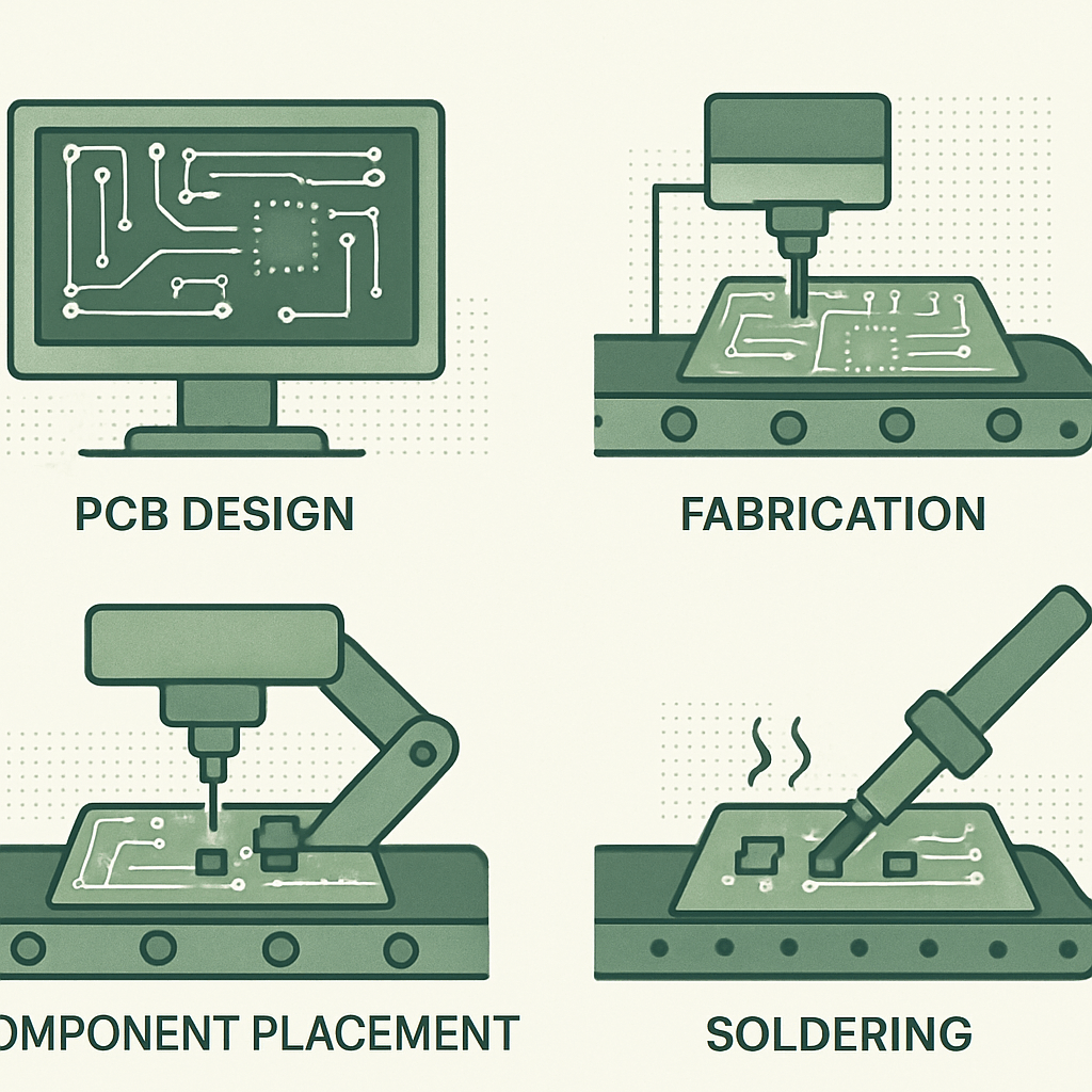
PCB assembly is the process of mounting electronic components onto a PCB. This involves several steps, including designing the PCB, fabricating the board, and soldering components onto it. The goal is to create a functional electronic circuit that can perform specific tasks.
Before any assembly can begin, a PCB must be designed. This phase involves creating a blueprint for the board, specifying the placement of components, and designing the electrical connections.
The first step is designing the layout of the PCB. Engineers use specialized software to create a schematic that represents the electronic circuit. This schematic is then translated into a layout that shows where each component will be placed on the board. The layout must be carefully planned to ensure efficient electrical connections and minimize interference.
Once the layout is complete, a Bill of Materials (BOM) is created. The BOM lists all the components needed for the assembly, including resistors, capacitors, and integrated circuits. This document helps in procuring the necessary parts and serves as a reference during the assembly process.

After the design phase, the next step is manufacturing the PCB. This involves several processes to create the physical board.
Fabrication begins with the production of the PCB substrate, usually made from fiberglass or another insulating material. The design layout is transferred onto the substrate using a photolithographic process, which involves coating the board with a photosensitive material and exposing it to light through a mask of the design.
Once the design is transferred, the next step is etching. During this process, unwanted copper is removed to leave only the desired circuit pattern. This is typically done using a chemical solution that dissolves the excess copper, leaving behind the paths that will connect the electronic components.
The solder mask is applied to the board to protect the copper traces from environmental damage and to prevent solder bridges during component placement. The solder mask is usually a green coating that covers the board, leaving only the necessary pads exposed for soldering.

With the PCB manufactured, the next step is placing the components onto the board.
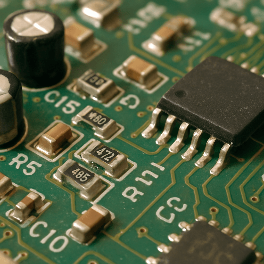
Surface Mount Technology (SMT) is the most common method for placing components on a PCB. In this process, components are placed directly onto the surface of the board. Automated machines pick and place components onto the board with high precision, ensuring accuracy and speed.
Through-hole technology involves placing component leads through pre-drilled holes in the board. This method is less common in modern electronics due to its complexity and the space it requires. However, it is still used for components that require a strong mechanical bond.

Soldering is the process of permanently attaching the components to the PCB. This is done by melting solder around the leads of the components and the pads on the board.
For SMT components, reflow soldering is the preferred method. The board, with components already placed, is passed through an oven where the solder paste melts and solidifies to form a strong bond between components and the board.
Wave soldering is used for through-hole components. In this method, the PCB is passed over a wave of molten solder, which coats the exposed metal and creates electrical connections. This process is efficient for mass production but requires careful control to prevent defects.
Once soldering is complete, the PCB undergoes inspection and testing to ensure functionality and reliability.
A visual inspection is performed to check for obvious defects such as misaligned components or solder bridges. This is often done using automated optical inspection (AOI) systems that can quickly identify issues.
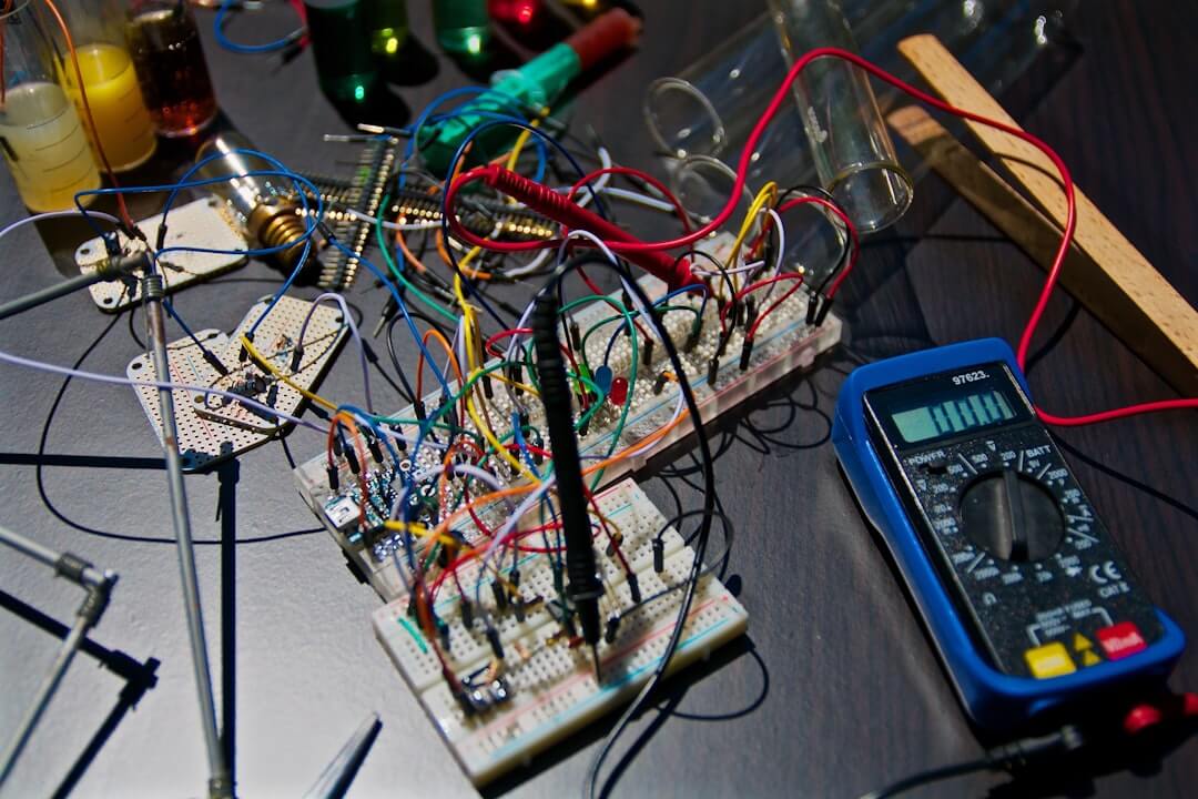
Functional testing involves checking the assembled PCB to ensure it performs the intended functions. This can include electrical tests to check connectivity and performance, as well as stress tests to ensure reliability under various conditions.
After passing inspection and testing, the PCB is ready for final assembly. This involves integrating the PCB into the final product, such as a smartphone or a computer.
The final step is integrating the assembled PCB into the device it was designed for. This may involve connecting the board to other components, such as displays or power sources, and securing it within a casing.
Understanding the PCB assembly process is crucial for anyone involved in electronics design and manufacturing. From designing the layout to final assembly, each step is essential for creating a reliable and functional electronic device. By following the processes outlined in this article, you can ensure a successful PCB assembly that meets your design requirements and performs as expected. Whether you are a hobbyist or a professional, grasping these fundamentals will enhance your ability to produce high-quality electronic products.

Got project ready to assembly? Contact us: info@apollopcb.com


We're not around but we still want to hear from you! Leave us a note:

Leave Message to APOLLOPCB
