-
- PCB TYPE
- PRINTED CIRCUIT BOARD PROTOTYPE ALUMINUM PRINTED CIRCUIT BOARD R&F PCB FPC HIGH FREQUENCY PCB HIGH-TG PCB HEAVY COPPER PCB HDI PCB PCB FOR LIGHTING METAL CORE PCB
time:Nov 19. 2025, 12:04:59
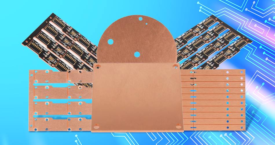
Thick Copper Sinkpad PCB Design has become an indispensable solution for high-power electronic systems demanding exceptional current-carrying capacity and thermal resilience. By integrating heavy copper layers (typically 1oz and above) with optimized sinkpad structures, this specialized design addresses the dual challenges of managing large electrical loads and dissipating concentrated heat—critical pain points in applications ranging from NEV charging modules to industrial power inverters. As electronic devices push toward higher power densities and compact form factors, Thick Copper Sinkpad PCB Design resolves the tradeoff between performance and reliability, outperforming standard copper-core PCBs in extreme operating conditions. This article explores the core design advantages, engineering principles, manufacturing precision, targeted applications, and future innovations of this advanced PCB technology.
The unique value of Thick Copper Sinkpad PCB Design lies in leveraging heavy copper’s material properties to deliver capabilities beyond standard PCB solutions.
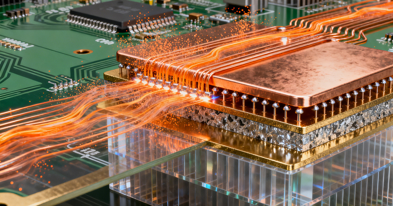
Thick copper layers provide significantly lower electrical resistance compared to standard copper foils, enabling the safe transmission of high currents without excessive power loss or overheating. Unlike conventional PCBs where thin copper traces restrict current flow, thick copper (≥35μm, per industry standards) minimizes voltage drop even in compact routing spaces. When paired with sinkpad structures, the heavy copper layer acts as both a current conduit and thermal pathway, supporting power-hungry components such as IGBTs and power MOSFETs in industrial and automotive systems. This dual functionality eliminates the need for separate bus bars, reducing system complexity and size.
Copper’s inherent thermal conductivity (401 W/(m·K))—69% higher than aluminum—combined with increased material volume in thick layers, delivers exceptional heat diffusion. The sinkpad’s direct thermal path (DTP) structure, integrated with heavy copper, accelerates heat transfer from component junctions to the PCB’s thermal management system. Unlike thin copper designs that concentrate heat in hotspots, thick copper layers spread thermal energy uniformly across the sinkpad, preventing localized temperature spikes that degrade component lifespan. This thermal resilience is critical for devices operating in sealed environments or extreme temperature ranges (-40°C to 125°C).
The increased thickness and density of heavy copper layers enhance the PCB’s structural rigidity, making it resistant to warping and vibration-induced damage. In harsh industrial or automotive environments, this mechanical robustness ensures consistent performance over extended thermal cycling. The sinkpad’s copper core, reinforced by thick circuit layers, forms a rigid platform that supports heavy components while maintaining thermal and electrical integrity. This durability reduces maintenance costs and improves reliability in mission-critical applications.

Designing effective Thick Copper Sinkpad PCBs requires balancing electrical, thermal, and mechanical requirements through targeted engineering strategies.
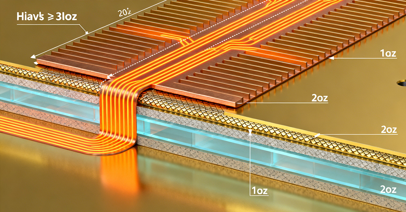
Engineers implement gradient copper thickness across the PCB to optimize performance: heavy copper (2–4oz) is allocated to high-current paths and sinkpad regions, while standard thicknesses are used for signal traces. This gradient minimizes material waste and weight while ensuring critical areas receive maximum current and thermal capacity. The sinkpad’s copper pedestal is strategically sized to match component thermal pads, with thick copper extensions radiating outward to enhance heat spreading. Thermal interface material (TIM) selection is tailored to the copper surface, ensuring minimal contact resistance without compromising electrical isolation.
Thick copper layers and sinkpad cores create thermal expansion mismatches with dielectric substrates, which can lead to delamination. To address this, designers integrate stress-relief features such as curved copper traces, dielectric buffer zones, and staggered via placement around sinkpad edges. These structures absorb thermal stress during temperature cycling, preventing structural failure. Additionally, the sinkpad’s thermoelectric separation architecture is preserved by isolating thick copper current paths from signal layers, ensuring electrical insulation while maintaining thermal continuity.
Despite the increased copper thickness, Thick Copper Sinkpad PCBs achieve high-density integration through optimized routing and via design. Blind/buried vias are used to connect thick copper layers without compromising thermal paths, while resin-filled vias reinforce mechanical stability. The sinkpad’s compact footprint, enabled by thick copper’s efficient heat and current handling, frees up space for additional components, supporting miniaturization in portable high-power devices.

Producing Thick Copper Sinkpad PCBs demands specialized processes to overcome the unique challenges of heavy copper fabrication.
Thick copper layers require stepwise etching to achieve uniform trace widths and avoid undercutting. Manufacturers use controlled etch chemistry and multiple pass etching to maintain tight tolerances, critical for high-current path accuracy. Hole metallization requires pre-treatment with strike current to ensure uniform copper deposition in via walls, preventing voids that compromise electrical and thermal conductivity. Surface finishes such as ENEPIG or immersion gold are applied to enhance solderability and corrosion resistance, extending operational lifespan.
The mismatched thermal expansion of thick copper and dielectric materials increases lamination complexity. Manufacturers employ vacuum lamination with precise temperature ramps to ensure full bonding without delamination. Warpage is controlled through symmetric layer stacking and pre-lamination stress relief of copper sheets. Post-lamination flattening processes further ensure the PCB maintains flatness, critical for component mounting and thermal interface contact.
Rigorous quality control measures include X-ray inspection to verify via integrity and copper thickness uniformity, thermal imaging to detect hotspots, and current-carrying capacity testing. Manufacturers also perform thermal cycling tests (-40°C to 125°C) to validate mechanical stability, ensuring the PCB meets industry reliability standards for high-power applications.

Thick Copper Sinkpad PCB Design is tailored to industries where high current and thermal management are non-negotiable.
In EV powertrains and charging systems, Thick Copper Sinkpad PCBs handle the high currents of battery management systems (BMS) and traction inverters. The design’s thermal resilience ensures reliable operation in under-hood environments, while its high-current capacity supports fast-charging capabilities. Additionally, the mechanical stability resists vibration and thermal cycling, extending the lifespan of critical automotive electronics.
Industrial inverters, motor drives, and power converters rely on Thick Copper Sinkpad PCBs to manage large currents and dissipate heat from high-power semiconductors. The design’s ability to minimize voltage drop improves energy efficiency, while uniform thermal diffusion prevents component overheating in 24/7 operating environments. This reliability reduces downtime and maintenance costs in manufacturing and automation systems.
Data center servers and high-performance computing (HPC) systems use Thick Copper Sinkpad PCBs to power dense CPU/GPU arrays. The thick copper layers handle the high current demands of power delivery networks (PDNs), while the sinkpad structure dissipates heat from concentrated compute loads. This enables higher compute densities without compromising thermal management, supporting the growth of AI and cloud computing infrastructure.

The evolution of Thick Copper Sinkpad PCB Design is driven by advancements in materials, manufacturing, and application demands.
Emerging copper-aluminum composite thick layers combine copper’s conductivity with aluminum’s lightweight properties, reducing PCB weight by up to 30% while maintaining performance. This innovation is critical for weight-sensitive applications such as aerospace and portable power devices. Graphene-enhanced thick copper further boosts thermal conductivity, enabling even more compact high-power designs.
Artificial intelligence tools are increasingly used to optimize thick copper routing and sinkpad placement. These tools simulate current flow, thermal diffusion, and mechanical stress simultaneously, generating designs that minimize material usage while maximizing performance. Machine learning algorithms predict potential failure points, allowing engineers to refine layouts before fabrication, reducing development cycles.
The industry is adopting eco-friendly processes for Thick Copper Sinkpad PCBs, including recycled copper materials and lead-free plating technologies. Energy-efficient etching and lamination processes reduce carbon footprint, while the design’s durability supports circular economy principles by extending product lifespans. These advancements align with global sustainability goals without compromising performance.
Thick Copper Sinkpad PCB Design represents a critical advancement in high-power electronic engineering, delivering unmatched current-carrying capacity, thermal resilience, and mechanical stability. By leveraging heavy copper layers and optimized sinkpad structures, this technology addresses the core challenges of modern high-power systems, enabling innovation in automotive, industrial, and computing industries. The careful balance of electrical, thermal, and mechanical design principles, combined with specialized manufacturing processes, ensures reliable performance in extreme operating conditions. As materials and design tools continue to advance, Thick Copper Sinkpad PCB Design will remain a cornerstone of high-power electronics, powering the next generation of efficient, compact, and sustainable devices.

Got project ready to assembly? Contact us: info@apollopcb.com


We're not around but we still want to hear from you! Leave us a note:

Leave Message to APOLLOPCB
