-
- PCB TYPE
- PRINTED CIRCUIT BOARD PROTOTYPE ALUMINUM PRINTED CIRCUIT BOARD R&F PCB FPC HIGH FREQUENCY PCB HIGH-TG PCB HEAVY COPPER PCB HDI PCB PCB FOR LIGHTING METAL CORE PCB
time:Jul 08. 2025, 09:53:32
In the rapidly evolving landscape of electronic design, prototyping plays a critical role in transforming conceptual ideas into functional solutions. Among the diverse range of printed circuit board (PCB) technologies, 2 layer aluminum PCBs have emerged as a preferred choice for prototyping applications that demand a balance of thermal efficiency, mechanical robustness, and cost - effectiveness. This article explores the engineering principles, design considerations, manufacturing processes, and real - world applications of 2 layer aluminum PCB prototypes, providing insights into their role in modern electronic development.
Fundamentals of 2 Layer Aluminum PCBs
Structural Overview
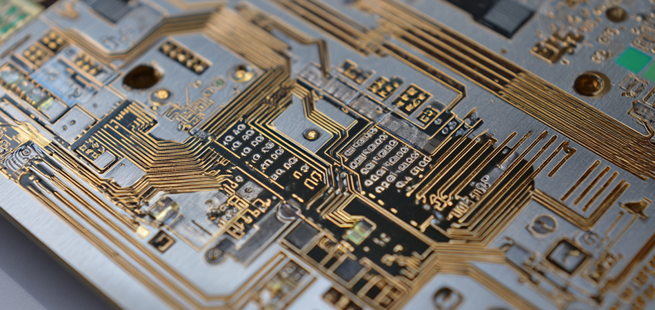
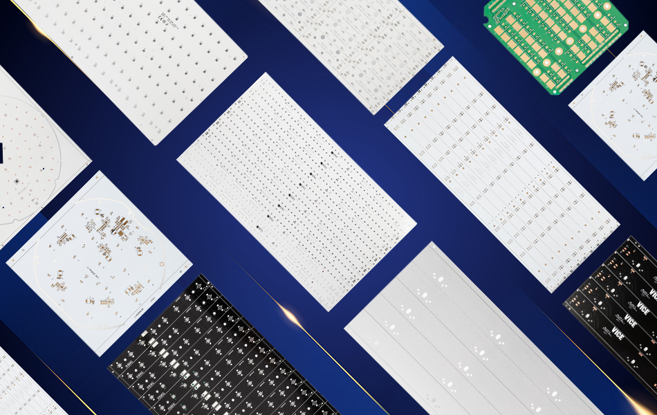
A 2 layer aluminum PCB prototype consists of two primary conductive layers—top and bottom—separated by a dielectric layer bonded to an aluminum substrate. The aluminum base serves as both a mechanical support and a thermal dissipater, while the two copper layers handle signal transmission and power distribution. This simple yet effective structure makes it ideal for applications where moderate complexity and efficient heat management are required without the added cost and complexity of multi - layer designs.
The aluminum substrate, typically composed of alloys like 6xxx series, offers a combination of high thermal conductivity and mechanical strength. The dielectric layer, often a ceramic - filled epoxy or polyimide, provides electrical insulation while facilitating heat transfer from the copper traces to the aluminum base. This dual - layer configuration strikes a balance between performance and simplicity, making it a versatile choice for prototyping across industries.
Key Advantages for Prototyping
Thermal Efficiency: The aluminum substrate efficiently dissipates heat generated by components, preventing thermal stress that could compromise prototype functionality during testing. This is particularly important for power - intensive components like LEDs, voltage regulators, or microprocessors.
Cost - Effectiveness: Compared to multi - layer PCBs, 2 layer designs reduce material and manufacturing costs, making them suitable for initial design iterations where budget and time are critical.
Design Flexibility: The two - layer layout allows for straightforward component placement and trace routing, enabling rapid design modifications during the prototyping phase.
Mechanical Durability: The aluminum substrate provides robust mechanical support, resisting bending and vibrations, which is essential for prototypes tested in real - world environments.
Design Considerations for 2 Layer Aluminum PCB Prototypes
Thermal Management Strategies
Component Placement
In 2 layer aluminum PCB prototypes, heat - generating components should be positioned on the top layer, directly above the aluminum substrate, to maximize heat transfer. Thermal vias—through - holes connecting the top copper layer to the aluminum base—are strategically placed around these components to create direct thermal pathways. The density and size of vias are optimized based on the component's power dissipation, with larger or more numerous vias used for higher - power devices.
Heat Sink Integration
For applications requiring enhanced thermal performance, the bottom layer of the PCB can be used to mount heat sinks or thermal pads. The aluminum substrate acts as a natural heat spreader, distributing heat across the board and into the heat sink, which is particularly effective in prototyping high - power LED fixtures or small - scale power supplies.
Electrical Design Principles
Trace Routing
In a 2 layer design, the top layer is typically used for signal traces and components, while the bottom layer serves as a ground plane or power distribution layer. This separation reduces electromagnetic interference (EMI) and provides a stable reference for signal integrity. High - speed signals should be routed on the top layer with controlled impedance, while the bottom layer's solid ground plane helps minimize noise.
Power Distribution
Power traces on the top layer are designed with sufficient width to handle the required current, avoiding voltage drops and excessive heating. The bottom layer can be used for distributing ground signals or low - voltage power, creating a balanced power - ground plane that improves overall circuit stability.
Mechanical Design Factors
Substrate Thickness
The thickness of the aluminum substrate is chosen based on the prototype's mechanical and thermal requirements. A thicker substrate offers greater mechanical strength and heat capacity, while a thinner substrate allows for more compact designs, suitable for portable or space - constrained applications.
Mounting and Form Factor
Mounting holes are incorporated into the design to secure the prototype within enclosures or test fixtures. The form factor—size and shape of the PCB—is optimized for the target application, with considerations for edge clearance, component spacing, and compatibility with mechanical interfaces.
Dielectric Layer Selection
Ceramic - filled epoxies are often preferred for dielectric layers in 2 layer prototypes due to their cost - effectiveness and balanced thermal - electrical properties. They offer better thermal conductivity than traditional FR4 dielectrics, ensuring efficient heat transfer to the aluminum substrate while providing adequate electrical insulation for most prototyping needs. Polyimide dielectrics may be used for high - temperature prototypes, such as those tested in industrial or automotive environments.
Manufacturing Processes for 2 Layer Aluminum PCB Prototypes
Design and Layout
CAD Tools
Designers use specialized software like Altium Designer, KiCad, or Eagle to create 2 layer layouts, ensuring proper component placement, trace routing, and thermal via positioning. These tools allow for thermal simulation to predict heat distribution and make iterative design improvements before manufacturing.
Gerber File Preparation
Gerber files, containing detailed layer information, are generated and verified for accuracy. Special attention is paid to thermal via placement and pad shapes to ensure proper heat dissipation and component soldering.
Material Preparation
Aluminum Substrate Cutting
The aluminum substrate is cut to the specified dimensions using CNC milling or laser cutting, ensuring precise edges and hole placement. The surface is cleaned and prepared to ensure proper adhesion of the dielectric layer and copper foil.
Dielectric Layer Lamination
A pre - cured dielectric sheet, either a ceramic - filled epoxy or polyimide, is laminated to the aluminum substrate using high - pressure and temperature processes. This creates a stable base for the copper layers, ensuring uniform thickness and thermal conductivity.
Copper Layer Fabrication
Copper Foil Lamination
Copper foil is laminated to both sides of the dielectric - coated aluminum substrate. The foil thickness is selected based on current requirements, with thicker foil used for power - intensive prototypes.
Photolithography and Etching
Photolithography is used to transfer the circuit design onto the copper foil. The exposed copper is etched away using chemical solutions, leaving the desired trace patterns on both the top and bottom layers. This process requires precision to ensure accurate trace widths and spacing, especially for fine - pitch components.
Via and Hole Formation
Drilling and Plating
Thermal vias and mounting holes are drilled using mechanical or laser drilling. Mechanical drilling is suitable for larger holes, while laser drilling offers precision for small vias. After drilling, the holes are plated with copper to ensure electrical connectivity between the top and bottom layers, with special attention to thermal vias to maximize heat transfer.
Surface Finishing
Options for Prototyping
Organic Solderability Preservative (OSP): A cost - effective option for prototyping, providing a thin organic layer that protects copper from oxidation and ensures good solderability.
Electroless Nickel Immersion Gold (ENIG): Used for prototypes requiring high - reliability connections, such as those with fine - pitch components or exposed contacts.
Hot Air Solder Leveling (HASL): A traditional finish suitable for prototypes where cost and ease of soldering are priorities.
Prototyping-Specific Considerations
Rapid prototyping services often use accelerated manufacturing processes, such as:
Laser Direct Imaging (LDI): For faster and more accurate pattern transfer, reducing lead times for small - batch prototypes.
Quick - Turn Lamination: Specialized presses that cure dielectric layers in shorter cycles, ideal for urgent prototype orders.
Quality Assurance for 2 Layer Aluminum PCB Prototypes
Electrical Testing
Continuity and Shorts
Using automated test equipment (ATE) or manual multimeters, engineers verify that there are no open circuits or short circuits between layers or traces. This is critical for ensuring the prototype's basic functionality before component assembly.
Impedance Matching
For high - speed signals, impedance testing ensures that trace widths and dielectric thicknesses match the designed impedance values, minimizing signal reflections and distortion.
hermal Testing
Infrared Thermography
Infrared cameras are used to map temperature distribution on the prototype when powered, identifying hotspots and verifying the effectiveness of thermal vias and component placement. This helps engineers optimize the design for better heat dissipation in subsequent iterations.
Thermal Cycling
Prototypes are subjected to repeated temperature cycles (e.g., -40°C to +85°C) to test the durability of the aluminum substrate, dielectric layer, and solder joints, ensuring they can withstand operational temperature fluctuations.
Mechanical Testing
Bend and Vibration Tests
Mechanical tests evaluate the substrate's resistance to bending and vibrations, ensuring the prototype remains intact during handling and real - world use. This is particularly important for portable or automotive prototypes.
Mounting Stability
Testing the integrity of mounting holes and fixtures ensures the prototype can be securely installed in enclosures or test setups without mechanical failure.
Applications of 2 Layer Aluminum PCB Prototypes
LED Lighting Prototyping
Commercial and Residential Fixtures
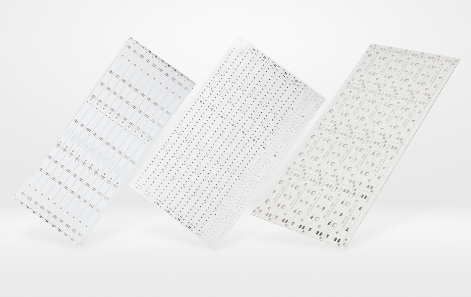
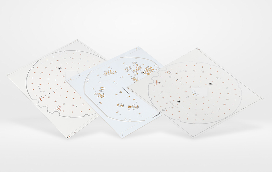
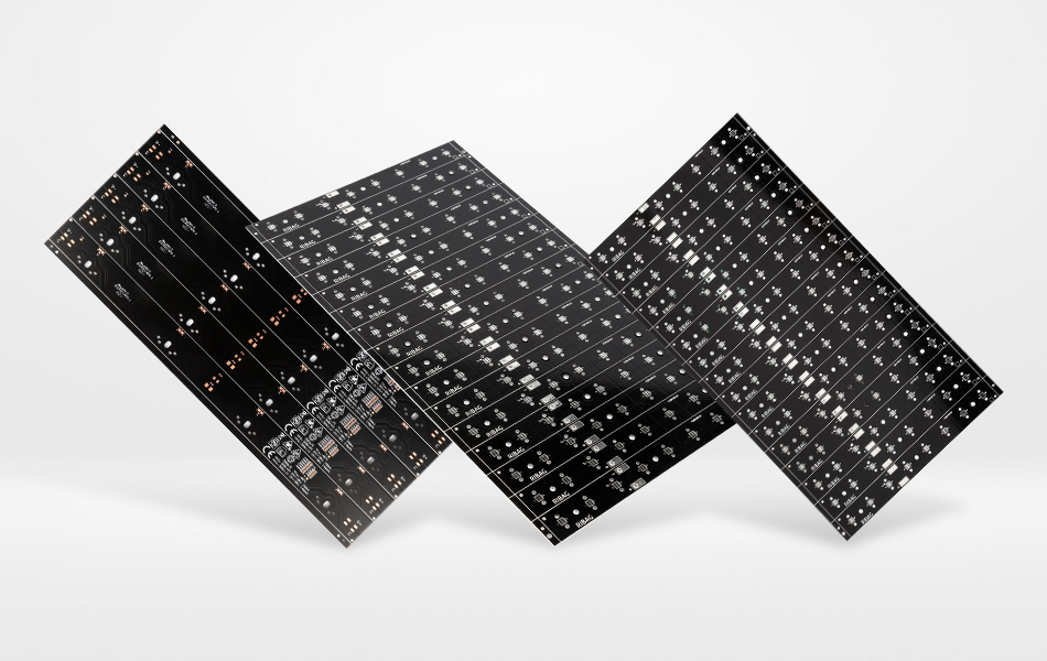
Prototypes for LED panels, downlights, or linear fixtures use 2 layer aluminum PCBs to manage heat from LED arrays. The two - layer design allows for straightforward placement of LEDs on the top layer, with the bottom layer serving as a heat sink interface, ensuring uniform light output and extended LED lifespan during testing.
Automotive Lighting
Prototypes for automotive taillights, headlights, or interior lighting leverage the aluminum substrate's vibration resistance and thermal efficiency. The two - layer layout simplifies the integration of LED drivers and thermal management components, critical for meeting automotive reliability standards.
Power Electronics Prototyping
DC - DC Converters
Prototypes for small - to - medium - power DC - DC converters use 2 layer aluminum PCBs to dissipate heat from power transistors and inductors. The bottom layer's ground plane provides a stable reference for high - frequency signals, while the aluminum substrate prevents overheating during load testing.
Battery Management Systems (BMS)
BMS prototypes for electric vehicles or energy storage systems rely on 2 layer aluminum PCBs to manage heat from battery monitoring circuits and power switches, ensuring safe and efficient operation during prototype validation.
Consumer Electronics Prototyping
Portable Devices
Prototypes for laptops, tablets, or wearable devices use 2 layer aluminum PCBs to balance thermal management and compact design. The aluminum substrate helps dissipate heat from processors or batteries, while the two - layer layout allows for efficient routing of high - speed data signals and power traces.
Audio Equipment
Audio amplifiers or soundbars use 2 layer aluminum prototypes to manage heat from power amplifiers, ensuring stable operation and reducing noise interference through proper ground plane design.
Industrial and IoT Prototyping
Industrial Controllers
Prototypes for motor controllers or sensor hubs in industrial automation use 2 layer aluminum PCBs to withstand harsh environments. The aluminum substrate's corrosion resistance and thermal efficiency are critical for maintaining performance in dusty, humid, or high - temperature settings.
IoT Sensors
Compact IoT sensor prototypes benefit from the lightweight and thermal properties of 2 layer aluminum PCBs, ensuring reliable operation in remote or space - constrained locations, such as smart city sensors or environmental monitoring devices.
Market Trends and Future Directions
Growing Demand for Rapid Prototyping
The rise of small - batch manufacturing and customized electronics has increased the demand for 2 layer aluminum PCB prototypes. Companies are leveraging these prototypes to quickly validate designs, reduce time - to - market, and minimize risks associated with mass production.
Integration with Advanced Materials
Future prototypes may incorporate advanced dielectric materials with higher thermal conductivity, such as boron nitride nanocomposites, to further enhance heat dissipation in 2 layer designs. These materials could enable smaller form factors for high - power prototypes without compromising performance.
Sustainable Prototyping Practices
Environmental concerns are driving the adoption of recycled aluminum substrates and eco - friendly dielectric materials in prototyping. Manufacturers are also implementing greener etching and plating processes to reduce the environmental impact of 2 layer aluminum PCB production.
Automation in Prototyping
Advanced automation tools, such as AI - powered design assistants and robotic assembly systems, are streamlining the prototyping process. These technologies reduce human error, accelerate design iterations, and enable real - time thermal and electrical simulations for more accurate 2 layer aluminum PCB prototypes.
Conclusion
2 layer aluminum PCB prototypes serve as a vital bridge between conceptual design and mass production, offering a balanced combination of thermal efficiency, cost - effectiveness, and design flexibility. Their role in prototyping spans diverse industries, from LED lighting and power electronics to consumer devices and industrial automation, enabling engineers to validate designs in real - world scenarios. As technology continues to advance, the integration of advanced materials, sustainable practices, and automation will further enhance the capabilities of 2 layer aluminum PCBs, solidifying their position as a cornerstone of modern electronic prototyping. By understanding their engineering fundamentals and practical applications, designers and manufacturers can leverage these prototypes to drive innovation and bring reliable, high - performance products to market efficiently.

Got project ready to assembly? Contact us: info@apollopcb.com


We're not around but we still want to hear from you! Leave us a note:

Leave Message to APOLLOPCB
