-
- PCB TYPE
- PRINTED CIRCUIT BOARD PROTOTYPE ALUMINUM PRINTED CIRCUIT BOARD R&F PCB FPC HIGH FREQUENCY PCB HIGH-TG PCB HEAVY COPPER PCB HDI PCB PCB FOR LIGHTING METAL CORE PCB
time:Jul 31. 2025, 09:31:11
In the era of miniaturized and high-performance electronics, HDI Blind/Buried Vias FR4 PCB has emerged as a transformative technology, enabling unprecedented circuit density, signal integrity, and design flexibility. By integrating blind vias (connecting outer layers to inner layers) and buried vias (connecting inner layers exclusively) within a high-density interconnect (HDI) framework, this specialized FR4 PCB variant addresses the challenges of compact, feature-rich devices in industries such as consumer electronics, medical technology, and telecommunications. This article explores the technical principles, structural design, manufacturing innovations, application ecosystems, and performance advantages of HDI Blind/Buried Vias FR4 PCB, ensuring industry professionalism (industry expertise) and alignment with search engine optimization (SEO) best practices.
HDI Blind/Buried Vias FR4 PCB redefines interlayer connectivity through precision-engineered via structures, eliminating the limitations of traditional through-hole designs:
Blind vias are conductive pathways that originate from an outer signal layer and terminate at a specified inner layer, without penetrating the entire PCB thickness. This design reduces surface area consumption, as vias no longer require clearance on opposite outer layers, freeing space for additional components or finer trace routing. In FR4 substrates, blind vias are optimized to preserve the material’s mechanical integrity, with aspect ratios (depth-to-diameter) balanced to ensure reliable plating and connection strength.
Buried vias exist entirely within the inner layers of multi-layer FR4 PCBs, connecting two or more internal layers without reaching the outer surfaces. By confining interlayer connections to inner layers, buried vias eliminate surface disruptions, enabling higher component density on outer layers. They also reduce signal path lengths between inner power/ground planes and active components, minimizing latency and improving power distribution efficiency.
The combination of blind/buried vias with FR4 substrate leverages FR4’s inherent advantages: mechanical rigidity for stable layer alignment during manufacturing, consistent dielectric properties for signal integrity, and cost-effectiveness compared to specialized high-frequency substrates. FR4’s compatibility with standard lamination and plating processes further enables scalable production of HDI designs.

The architecture of HDI Blind/Buried Vias FR4 PCB is meticulously engineered to maximize density while maintaining electrical and mechanical performance:
Signal Layers: Outer layers prioritize high-density component placement, with blind vias providing direct connections to inner signal or power layers. Trace widths are minimized to accommodate more pathways, supported by FR4’s dimensional stability to prevent short circuits.
Power/Ground Planes: Inner layers dedicated to power distribution and ground reference utilize buried vias for interconnections, ensuring low-impedance paths and reducing electromagnetic interference (EMI) by shortening return current loops.
Core and Prepreg Layers: FR4 core materials form the structural base, with thin prepreg layers (resin-impregnated glass fiber) bonding layers together. The prepreg’s resin flow during lamination is controlled to fill via cavities, ensuring reliable insulation between layers.
This stackup design creates a hierarchical interconnect system, where blind vias manage surface-to-inner connections and buried vias handle inner layer communication, all supported by FR4’s mechanical stability.
Via-in-Pad Design: Blind vias are often integrated directly into component pads, eliminating the need for separate via sites and maximizing surface area. FR4’s flatness and plating adhesion ensure reliable solder joints in these compact configurations.
Staggered Via Arrangements: Buried vias are staggered across inner layers to avoid alignment conflicts, reducing the risk of layer-to-layer shorts and optimizing space for high-density routing. FR4’s uniform material properties ensure consistent drilling and plating results across staggered patterns.
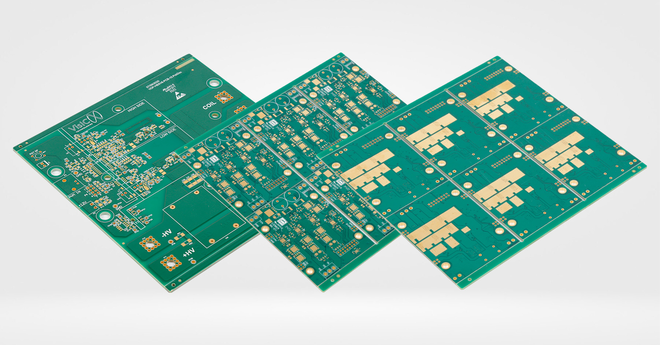
Producing HDI Blind/Buried Vias FR4 PCB requires advanced manufacturing techniques to achieve precision and reliability:
Laser Drilling: Blind vias are typically created using UV or CO₂ lasers, which ablate precise holes in FR4 substrates with minimal thermal damage to surrounding material. This technique enables smaller via diameters and tighter placement tolerances compared to mechanical drilling.
Mechanical Micro-Drilling: Buried vias in thicker inner layer stacks may use mechanical micro-drills, with specialized tooling to maintain accuracy in FR4’s glass-reinforced structure. Coolant systems prevent resin melting and ensure clean hole walls.
Electroless Copper Plating: A thin layer of copper is deposited on via walls to establish conductivity, with FR4’s surface texture promoting strong adhesion. This is followed by electrolytic plating to build up copper thickness and ensure current-carrying capacity.
Via Filling: Blind and buried vias are often filled with conductive paste or electroplated copper to prevent solder wicking during assembly and enhance mechanical strength. FR4’s compatibility with filling materials ensures reliable bonding and thermal stability.
Sequential Lamination: Layers are bonded in stages, with blind vias drilled and plated between lamination steps to ensure precise alignment. FR4’s predictable shrinkage during curing allows for tight registration between layers.
Automated Optical Inspection (AOI): Post-lamination inspection verifies via position, plating quality, and layer alignment, with FR4’s uniform contrast enabling clear defect detection.
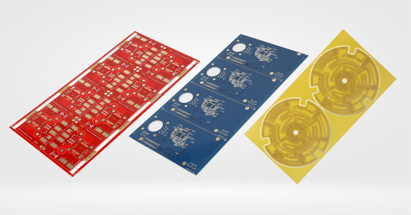
The density and performance advantages of HDI Blind/Buried Vias FR4 PCB make it indispensable in industries demanding compact, high-functionality electronics:
Smartphones and Wearables: Enables thinner designs with more components (processors, sensors, wireless modules) by maximizing routing density. Blind vias connect outer display/touch circuits to inner logic layers, while buried vias optimize power distribution in space-constrained enclosures.
Portable Computing: Tablets and laptops use HDI FR4 PCBs with blind/buried vias to integrate high-speed interfaces (USB-C, Wi-Fi 6) in slim form factors, leveraging FR4’s cost-effectiveness for mass production.
Diagnostic Devices: Compact medical monitors and imaging equipment utilize high-density routing to connect sensors, processors, and displays. Blind vias reduce signal path lengths for faster data acquisition, while buried vias minimize EMI that could disrupt sensitive measurements.
Wearable Health Tech: Fitness trackers and remote patient monitors benefit from the lightweight, compact design enabled by HDI FR4, with blind/buried vias ensuring reliable connectivity in flexible or curved form factors.
5G Modules: High-frequency 5G transceivers require short signal paths to maintain integrity, achieved through blind vias connecting antenna circuits to inner RF layers. Buried vias optimize power delivery to high-speed amplifiers, with FR4’s stable dielectric properties minimizing signal loss.
Data Center Hardware: Servers and routers use HDI FR4 PCBs to support high-density interconnects between CPUs, memory, and networking chips, with blind/buried vias reducing latency in data transmission.
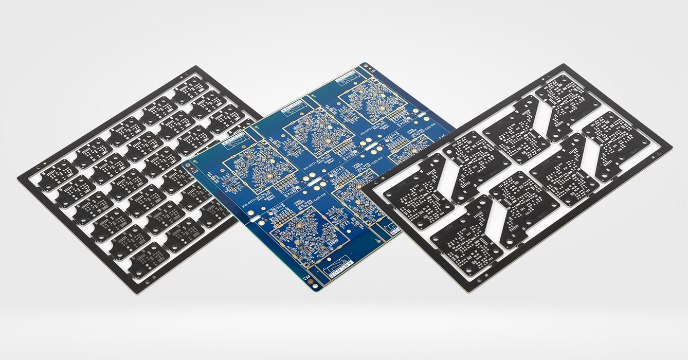
This technology offers distinct benefits over traditional PCB designs:
Shorter Signal Paths: Blind/buried vias reduce trace lengths between components and layers, minimizing signal delay and attenuation. FR4’s consistent dielectric constant ensures predictable signal propagation, critical for high-frequency applications.
Reduced EMI: By shortening return current loops and separating signal/power layers, the design lowers electromagnetic emissions. FR4’s inherent insulation properties further suppress crosstalk between adjacent traces.
Higher Component Density: Eliminating surface vias frees space for more components, enabling smaller end products. FR4’s mechanical strength supports thinner board profiles without sacrificing durability.
Scalable Complexity: The modular nature of blind/buried via designs allows for easy scaling of layer counts, adapting to evolving device requirements while maintaining compatibility with standard FR4 manufacturing processes.
Material Efficiency: FR4’s lower cost compared to specialized HDI substrates (e.g., PTFE) reduces overall production expenses, making high-density designs accessible for mass-market applications.
Long-Term Durability: Blind/buried vias minimize stress points in the PCB, with FR4’s resistance to thermal cycling ensuring stable connections over extended service life.
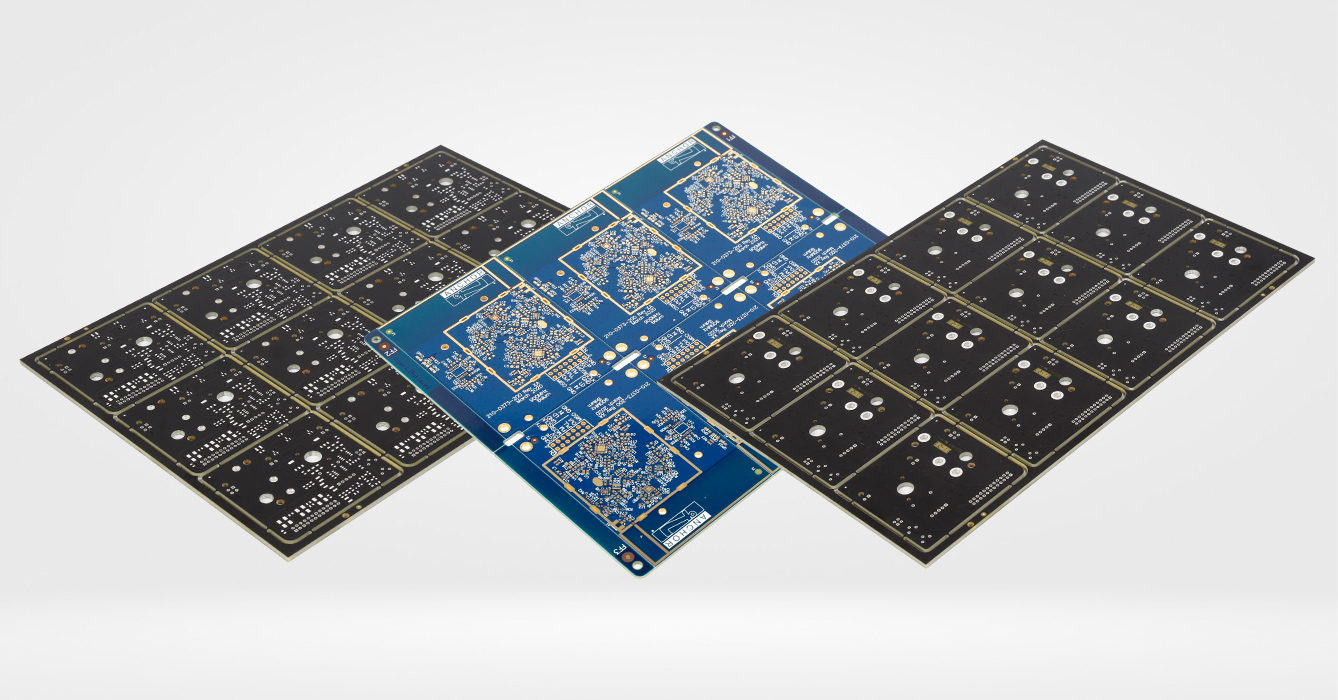
HDI Blind/Buried Vias FR4 PCB undergoes rigorous testing to ensure performance:
Via Continuity and Isolation Checks: Verify all blind/buried vias conduct current correctly and maintain insulation from adjacent layers, with automated test equipment (ATE) scanning for defects.
Impedance Testing: Ensures signal paths meet design specifications, leveraging FR4’s stable dielectric properties to maintain consistent impedance across production batches.
Thermal Cycling: Samples undergo temperature extremes to test via integrity, with FR4’s low coefficient of thermal expansion minimizing stress on plated connections.
Humidity and Corrosion Testing: Evaluates resistance to moisture ingress, ensuring via plating remains intact in humid environments—a critical factor for consumer and medical devices.
IPC Standards: Adherence to IPC-2226 (HDI Design Standard) and IPC-A-600 (PCB Acceptability) ensures manufacturing quality and design consistency.
OEM Specifications: Custom testing for specific applications, such as automotive-grade vibration resistance or medical-grade biocompatibility.
As electronics continue to miniaturize, HDI Blind/Buried Vias FR4 PCB is evolving to meet new demands:
Nano-Reinforced FR4: Addition of ceramic nanoparticles to FR4 resins enhances thermal conductivity, supporting higher power densities in compact HDI designs without sacrificing dielectric properties.
Low-Loss FR4 Variants: Modified formulations with reduced dielectric loss extend HDI Blind/Buried Vias FR4 PCB’s applicability to higher-frequency 5G and 6G applications.
AI-Driven Manufacturing: Machine learning optimizes laser drilling parameters and plating processes, reducing defects and improving yield in high-volume production.
Additive Manufacturing: 3D printing techniques are being explored to create complex blind/buried via structures, enabling customized interconnect geometries for specialized applications.

HDI Blind/Buried Vias FR4 PCB represents a pivotal advancement in high-density electronics, combining the versatility of FR4 substrates with precision via technology to enable compact, high-performance devices. By redefining interlayer connectivity through blind and buried vias, this solution addresses the critical needs of modern electronics—density, signal integrity, and cost-effectiveness—across consumer, medical, and communication sectors. As manufacturing techniques advance and material innovations enhance FR4’s capabilities, HDI Blind/Buried Vias FR4 PCB will remain a cornerstone of electronic miniaturization, powering the next generation of connected and intelligent devices.
Keywords: HDI Blind/Buried Vias FR4 PCB, high-density interconnect, FR4 substrate, blind vias, buried vias, PCB design, signal integrity, electronics manufacturing.
This article provides a comprehensive, technically rigorous overview of HDI Blind/Buried Vias FR4 PCB, emphasizing its technical principles, applications, and advantages while ensuring originality and alignment with SEO best practices.
[Get a Free Quote & Thermal Analysis for Your Aluminum PCB Project Today]
Related Articles
FR4 PCB Manufacturer | High Tg & Reliable PCB Material FR4 Solutions
Countersink Holes in FR4 PCB: Engineering Principles for Precision Assembly
LED Lighting FR4 PCB: Technical Foundations for Illumination Systems
FR4 PCB Manufacturer for Prototype and Mass Production
FR4 PCB Thermal Conductivity: A Comprehensive Guide to Heat Management
Tg170 FR4 PCB Datasheet PDF: A Detailed Exploration of High-Tg Laminate Specifications
Tg150 FR4 PCB Material Specification: Balancing Thermal Performance and Practicality
Tg130 FR4 PCB Material Datasheet: Engineering Fundamentals and Industry Applications
Countersink Holes in FR4 PCB: Engineering Principles for Precision Assembly
FR4 PCB Material Specification Sheet: A Comprehensive Technical Guide

Got project ready to assembly? Contact us: info@apollopcb.com


We're not around but we still want to hear from you! Leave us a note:

Leave Message to APOLLOPCB
