-
- PCB TYPE
- PRINTED CIRCUIT BOARD PROTOTYPE ALUMINUM PRINTED CIRCUIT BOARD R&F PCB FPC HIGH FREQUENCY PCB HIGH-TG PCB HEAVY COPPER PCB HDI PCB PCB FOR LIGHTING METAL CORE PCB

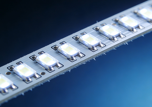
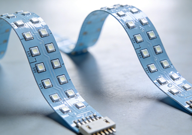
With the rapid expansion of high-performance lighting applications—from large-scale sports venues and new energy vehicle lighting to high-end commercial displays and medical surgical lighting—the demand for high brightness LED FPCB (Flexible Printed Circuit Board) has surged. A reliable High Brightness LED FPCB Manufacturer plays a pivotal role in this ecosystem, as it is not only a producer of core components but also a co-innovator that empowers downstream industries to achieve breakthroughs in lighting performance, design flexibility, and energy efficiency. Unlike ordinary LED FPCB manufacturers that focus solely on basic functionality, a professional High Brightness LED FPCB Manufacturer integrates advanced material technology, precision manufacturing processes, and customized solution capabilities to meet the stringent requirements of high-luminance, high-stability lighting scenarios. For enterprises engaged in lighting system design, automotive electronics, and display technology
Premium Waterproof LED FPCB manufacturer. Advanced IP67/IP68 protection for high-humidity & harsh lighting. UV-resistant, flexible & long-lasting. Secure your project with ApolloPCB—Request a quote!
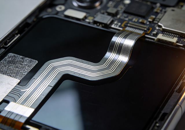
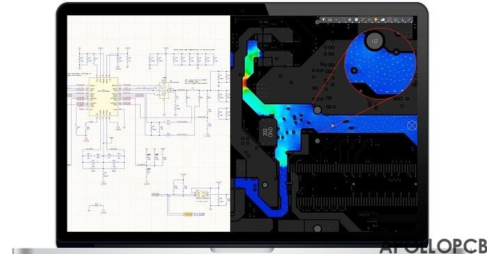
The relentless pursuit of smarter, more adaptive electronic devices has made Flexible Printed Circuit Board (FPCB) a transformative force in the electronics industry. Unlike traditional rigid PCBs that constrain device design to fixed shapes and sizes, FPCB introduces unprecedented flexibility, enabling engineers to reimagine product forms while enhancing performance and user experience. From ultra-thin wearables that conform to the human body to curved automotive interfaces that blend seamlessly with interior designs, FPCB has become the backbone of innovative electronic products across sectors. As consumer demand for portability, ergonomics, and multi-functionality grows, the role of FPCB in shaping the future of electronics continues to expand.
Enable extreme miniaturization with ApolloPCB’s Blind & Buried Vias FPCB. Optimize space & signal performance for wearables & high-density electronics. Reliable multi-layer flex circuits—Get a quote!
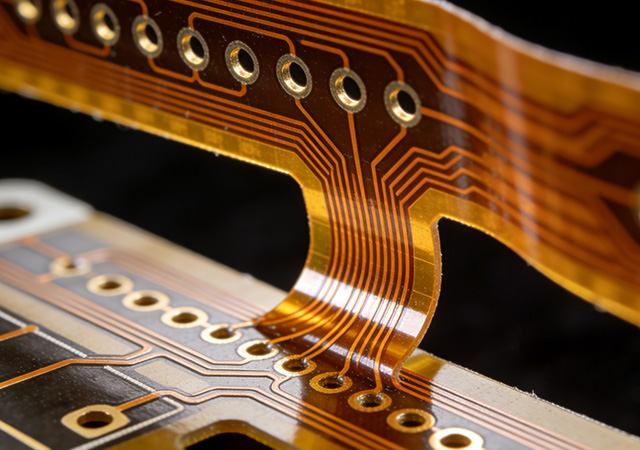
Boost RF performance with ApolloPCB’s Blind Vias FPCB. Minimize signal loss & stubs for 5G, IoT & radar systems. High-frequency precision engineering—Get your RF FPC quote now!

Got project ready to assembly? Contact us: info@apollopcb.com


 Whatsapp 0086 755 29438407
 Mail info@apollopcb.com
 Tel 0086 755 29438407


ABOUT US

PRODUCTS
TECHNOLOGY
KNOWLEDGE CENTRE
CULTURE
NEWS
We're not around but we still want to hear from you! Leave us a note:

Leave Message to APOLLOPCB