-
- PCB TYPE
- PRINTED CIRCUIT BOARD PROTOTYPE ALUMINUM PRINTED CIRCUIT BOARD R&F PCB FPC HIGH FREQUENCY PCB HIGH-TG PCB HEAVY COPPER PCB HDI PCB PCB FOR LIGHTING METAL CORE PCB
time:Jul 16. 2025, 09:41:53
Thermal vias represent a critical design element in aluminum printed circuit boards (PCBs), serving as strategic pathways to transfer heat from high-power components to aluminum substrates—nature’s efficient heat sinks. In applications ranging from industrial power supplies to automotive electronics, where thermal management directly impacts reliability and performance, optimizing thermal via structure is paramount. This comprehensive guide explores thermal via design principles, material interactions, manufacturing considerations, and application-specific strategies in aluminum PCB structures, equipping engineers with the knowledge to maximize heat dissipation efficiency.
| Design Variable | Standard Aluminum PCB | Apollo Optimized (Thermal Vias) | Improvement |
| Thermal Resistance ($R_{\theta}$) | 1.5 - 2.5 °C/W | 0.5 - 0.8 °C/W | 65% Reduction |
| Heat Transfer Efficiency | Passive (Dielectric) | Active (Copper Bridge) | 3x Faster |
| Component Lifespan | Standard | Extended by 40% | Significant |
| Current Carrying Capacity | Limited | High Power Ready | Reliable |
| Solder Wicking Risk | None | Prevented via Plugging | High Reliability |
Unlike signal vias, which prioritize electrical connectivity between layers, thermal vias are engineered explicitly for heat transfer:
Primary Function: Create low-resistance pathways for heat to flow from copper traces (where components generate heat) through dielectric layers to the aluminum substrate, which dissipates heat into the surrounding environment or attached cooling systems.
Structural Distinction: Typically larger in diameter and more densely packed than signal vias, thermal vias minimize thermal resistance at material interfaces—critical in aluminum PCBs where the aluminum core acts as the primary heat-dissipating component.
Electrical Neutrality: While some thermal vias double as ground connections, many are designed with non-conductive fillers to isolate signal layers, ensuring heat transfer without electrical interference.
In aluminum PCBs, thermal vias address two core challenges:
Hotspot Mitigation: Concentrated heat from components like power MOSFETs or LEDs can create localized hotspots (>150°C) that degrade performance. Thermal vias channel this heat away from components, reducing junction temperatures by 20–40% compared to non-vias designs.
Thermal Resistance Reduction: The dielectric layer in aluminum PCBs—while electrically insulating—acts as a thermal barrier. Thermal vias bypass this barrier, creating direct thermal paths between heat sources and the aluminum core, lowering overall thermal resistance by 30–50%.
Uniform Heat Distribution: Strategic via placement spreads heat across the aluminum substrate, preventing uneven thermal expansion that can cause solder joint fatigue or layer delamination.
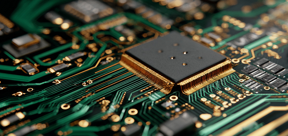
Thermal via placement is dictated by heat source location and substrate geometry:
Proximity to Heat Sources: Vias should be placed within 1–2mm of high-power components to minimize lateral heat spread through copper traces, which have higher thermal resistance than direct via pathways. This is critical for components like IGBTs in EV inverters, where even small distances increase junction temperatures.
Cluster vs. Distributed Patterns: For large heat sources (e.g., LED arrays), distributed vias (evenly spaced across the component footprint) ensure uniform heat extraction. For point sources (e.g., a single power transistor), clustered vias directly under the component create a concentrated thermal pathway.
Alignment with Aluminum Core Features: Vias should align with thick sections of the aluminum core or integrated heat sinks, avoiding areas with structural cutouts that reduce heat dissipation capacity.
Thermal via dimensions are optimized for heat flow, not just manufacturability:
Diameter Selection: Larger diameters (relative to signal vias) increase cross-sectional area for heat transfer, but must balance with PCB thickness to maintain structural integrity. In aluminum PCBs, via diameters are typically sized to match the thermal conductivity requirements of the application—higher-power devices demand larger or more numerous vias.
Aspect Ratio Limits: The ratio of via depth (PCB thickness) to diameter is kept below critical thresholds to ensure reliable plating and minimize thermal resistance. Excessive aspect ratios can lead to plating voids, creating bottlenecks in heat transfer.
Pitch Optimization: Via spacing (pitch) is designed to avoid overlapping thermal fields, ensuring each via contributes to heat extraction without redundancy. Overcrowded vias waste space and increase manufacturing costs without proportional gains in cooling.
Thermal via filling materials impact both heat transfer and mechanical stability:
Conductive Fillers: Epoxy or solder-based fillers with high thermal conductivity (≥2 W/mK) enhance heat transfer through the via, particularly in multi-layer aluminum PCBs where vias connect multiple copper layers to the aluminum core. Solder filling also improves mechanical strength, critical in vibration-prone environments like automotive electronics.
Plating Thickness: Thick copper plating (≥25μm) on via walls minimizes contact resistance between copper traces and the via, ensuring efficient heat flow. This is especially important in high-current aluminum PCBs, where resistive heating in vias can negate cooling benefits.
Non-Conductive Fillers: For vias near sensitive signal traces, non-conductive thermally conductive fillers (e.g., ceramic-loaded epoxies) prevent electrical shorting while maintaining heat transfer—essential in mixed-signal boards like industrial sensor controllers.
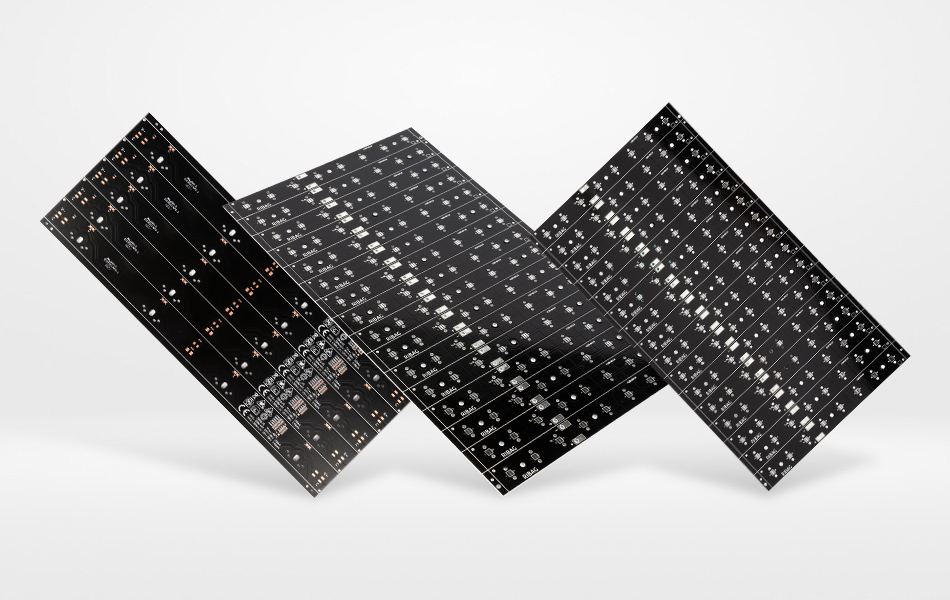
The dielectric layer between copper traces and the aluminum core influences via performance:
Thermal Resistance Matching: Dielectric materials with lower thermal resistance (e.g., ceramic-filled epoxies) reduce the barrier to heat flow from vias to the aluminum core. This is critical in high-frequency applications where low-loss dielectrics (e.g., PTFE blends) are used, as these often have lower thermal conductivity than standard epoxies.
Adhesion to Vias: Dielectrics must maintain strong adhesion to via plating and aluminum to prevent delamination during thermal cycling. Plasma treatment of via walls before dielectric application enhances bonding, reducing interface thermal resistance.
Thickness Trade-offs: Thinner dielectrics reduce thermal resistance between vias and the aluminum core but require higher dielectric strength to prevent breakdown in high-voltage applications (e.g., power distribution boards).
The aluminum substrate’s properties directly impact via effectiveness:
Alloy Thermal Conductivity: High-purity aluminum alloys (e.g., 1xxx series) or thermally enhanced 6xxx series alloys maximize heat spreading from via endpoints, ensuring heat from vias is quickly distributed across the substrate.
Surface Roughness: A micro-roughened aluminum surface increases contact area with the dielectric layer, enhancing heat transfer from vias to the core. This is achieved through chemical etching or anodization processes tailored for thermal performance.
Core Thickness: Thicker aluminum cores provide greater heat capacity, reducing temperature rise at via endpoints. However, they increase PCB weight, a consideration in aerospace or portable electronics.
Copper layers act as thermal highways between components and vias:
Trace Width Optimization: Wide, short copper traces from components to via clusters minimize thermal resistance, ensuring heat reaches vias before significant temperature drops occur. This is critical in high-current paths (e.g., battery management systems) where resistive heating in traces is substantial.
Plane vs. Trace Connections: Using a solid copper plane under heat sources, connected to vias, distributes heat across multiple vias simultaneously, reducing reliance on individual via performance. This is standard in power supply PCBs, where large copper planes act as both current carriers and heat spreaders.
Surface Finish Impact: Matte or textured copper finishes (vs. smooth) increase surface area for heat transfer to vias, though they must balance with solderability requirements for component mounting.
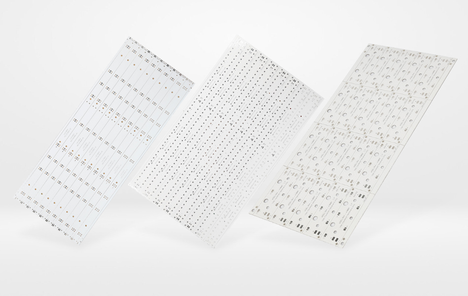
Precision manufacturing ensures thermal via reliability:
Laser vs. Mechanical Drilling: Laser drilling creates smaller, more precise vias for dense designs (e.g., 5G power amplifiers), while mechanical drilling is cost-effective for larger vias in industrial PCBs. Both methods require burr-free edges to prevent dielectric damage during lamination.
Plating Uniformity: Electroless copper plating followed by electrolytic plating ensures consistent wall thickness, avoiding thin spots that restrict heat flow. Automated optical inspection (AOI) verifies plating integrity, critical for high-reliability applications like medical devices.
Desmearing and Cleaning: Post-drilling desmearing removes dielectric residue from via walls, ensuring strong adhesion between plating and dielectric. This step is especially important for ceramic-filled dielectrics, which are prone to residue buildup.
Thermal via performance is validated through targeted testing:
Thermal Resistance Measurement: Using thermal transient analysis, engineers measure the resistance between the component pad and aluminum core, ensuring vias meet design targets. This is often paired with infrared (IR) thermography to visualize hotspot reduction.
Thermal Cycling Testing: PCBs undergo -40°C to +125°C cycles to test via integrity, with scanning acoustic microscopy (SAM) detecting delamination at via interfaces—a common failure mode in harsh environments.
Pressure Testing for Filled Vias: Filled vias are subjected to mechanical stress tests to ensure filler materials don’t crack or separate from walls, maintaining thermal conductivity over time.
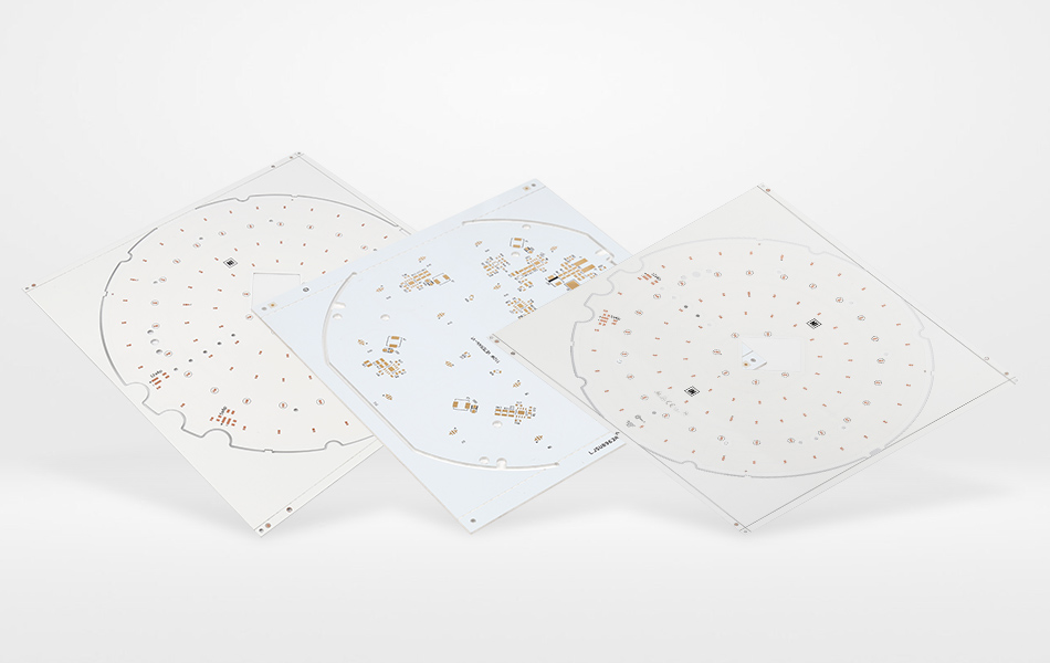
In automotive systems, thermal vias address extreme operating conditions:
Battery Management Systems (BMS): Vias under current sensors and balancing circuits dissipate heat in tight enclosures, preventing thermal runaway. Clustered vias connect to thick aluminum cores, which act as passive heat sinks.
ADAS Radar Modules: Small, dense vias in low-loss dielectric layers remove heat from high-frequency MMICs (monolithic microwave integrated circuits), ensuring stable performance in temperature-fluctuating under-hood environments.
Thermal vias enable reliable operation in high-power industrial settings:
Motor Drives: Large-diameter vias under IGBTs and diodes transfer heat to aluminum-backed heat sinks, supporting continuous operation at 100% load. Filled vias with solder enhance thermal and mechanical stability in vibration-prone factory floors.
PLCs and Industrial Controllers: Distributed vias across power supply sections prevent overheating in enclosed control cabinets, where active cooling is limited.
Thermal vias extend lifespan in lighting applications:
High-Bay LED Fixtures: Vias under LED arrays connect to aluminum cores with integrated fins, dissipating heat to prevent lumen depreciation. Distributed via patterns ensure each LED chip operates within safe temperature ranges.
UV-C Disinfection Systems: Heat-sensitive UV LEDs rely on thermal vias to maintain efficiency, with vias placed strategically to avoid shadowing light output while maximizing heat extraction.
Designers must navigate trade-offs:
Via Count Optimization: Increasing via count improves heat transfer but raises manufacturing costs. Simulation tools (e.g., CFD software) help identify the minimum via count needed to meet thermal targets, avoiding over-engineering.
Material Selection Costs: High-thermal-conductivity fillers and thick plating increase costs but are justified in reliability-critical applications (e.g., aerospace). For consumer electronics, standard fillers with moderate thermal performance balance affordability and functionality.
Advancements in thermal via technology include:
3D-Printed Via Structures: Additive manufacturing enables complex via geometries (e.g., tapered vias with larger endpoints) that reduce thermal resistance without increasing diameter.
Embedded Thermal Sensors: Vias integrated with thin-film sensors monitor real-time temperature at heat sources, enabling adaptive cooling in smart systems like data center power supplies.
Graphene-Enhanced Plating: Graphene-infused copper plating increases via thermal conductivity by 20–30%, supporting higher power densities in next-gen electronics.
Thermal vias are indispensable in unlocking the full potential of aluminum PCBs, bridging the gap between high-power components and the aluminum core’s heat-dissipating capabilities. By following strategic placement, sizing, and material guidelines, engineers can design thermal via structures that reduce hotspots, enhance reliability, and enable miniaturization in heat-constrained applications. As industries like automotive electrification and renewable energy demand ever-higher power densities, thermal via innovation will remain critical—ensuring aluminum PCBs continue to deliver efficient, durable performance where traditional PCBs fall short. For engineers, mastering thermal via design in aluminum PCBs is not just a technical skill but a key enabler of next-generation electronic systems.
Related Articles
Aluminum PCB Manufacturer | High Thermal Conductivity MC-PCB Boards
HA80 Aluminum PCB Specifications: Technical Foundations and Industrial Adaptability
GDM Aluminum Based CCL: A Versatile Foundation for Modern Electronics
Ventec Aluminum CCL Material Datasheet: A Paradigm of Thermal and Electrical Excellence
Boyu Aluminum CCL: Comprehensive Solutions for Advanced Electronics
Aluminium-Based CCL: Innovations in High-Performance Copper Clad Laminates
Aluminum PCB: Benefits and Applications for High-Power Electronics
Countersink Holes PCB Manufacturer: Precision & Quality
Aluminum PCB: Benefits and Applications for High-Power Electronics

Got project ready to assembly? Contact us: info@apollopcb.com


We're not around but we still want to hear from you! Leave us a note:

Leave Message to APOLLOPCB
