-
- PCB TYPE
- PRINTED CIRCUIT BOARD PROTOTYPE ALUMINUM PRINTED CIRCUIT BOARD R&F PCB FPC HIGH FREQUENCY PCB HIGH-TG PCB HEAVY COPPER PCB HDI PCB PCB FOR LIGHTING METAL CORE PCB

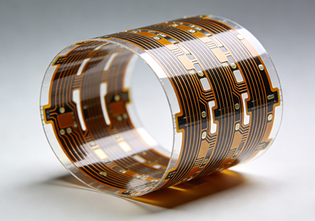
In the era of electronic innovation dominated by miniaturization, intelligence, and adaptability, FPCB (Flexible Printed Circuit Board) has evolved from a supporting component to a core connector that underpins the entire flexible electronics ecosystem. Unlike rigid PCBs that limit product form and application scenarios, FPCB’s unique flexibility, lightweight nature, and reliable electrical performance have broken through traditional design boundaries. It serves as a critical bridge between electronic components, enabling seamless integration of diverse technologies in fields such as consumer electronics, industrial IoT, and smart healthcare. As global demand for flexible, portable, and intelligent electronic products surges, FPCB’s role in driving industry upgrading and technological innovation becomes increasingly irreplaceable.

Unlock innovation with custom FPCB solutions. From material selection to complex multi-layer stack-ups. Learn how ApolloPCB’s 10-year technical team tailors flexible circuits for medical, automotive, and aerospace applications. Request your custom FPC quote today.
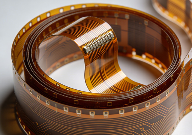
In the era of high-end electronics pursuing extreme performance and environmental adaptability, Polyimide Customize FPCB Solution has emerged as a core enabler for technological innovation. Polyimide, known as the "golden film" in the electronic material field, boasts exceptional thermal stability, electrical insulation, and environmental resistance. Combined with customized flexible printed circuit board (FPCB) design, this solution effectively addresses the pain points of traditional FPCB materials that struggle to withstand harsh conditions such as high temperatures, strong radiation, and chemical corrosion. From aerospace equipment operating in extreme cosmic environments to precision medical devices requiring long-term stable operation, Polyimide Customize FPCB Solution provides tailored, high-reliability circuit solutions, becoming an indispensable cornerstone for high-end electronic products.
Accelerate your R&D with ApolloPCB’s Quick Turn Customize FPCB service. High-quality prototypes in as little as 24-48 hours. From DFM to fabrication—Shorten your time-to-market today!
Flexible Printed Circuit Board (FPCB) has emerged as a transformative technology that is reshaping the landscape of modern electronics. Moving beyond the limitations of rigid printed circuit boards, FPCB’s inherent flexibility, miniaturization potential, and reliable electrical performance have made it a cornerstone of innovative product development across industries. From ultra-thin wearable devices that conform to the human body to complex flexible displays that redefine user interaction, FPCB is driving a paradigm shift in how electronic devices are designed, manufactured, and experienced. As the demand for smarter, more adaptive electronics continues to surge, FPCB’s role in enabling technological advancement becomes increasingly indispensable.

Got project ready to assembly? Contact us: info@apollopcb.com


 Whatsapp 0086 755 29438407
 Mail info@apollopcb.com
 Tel 0086 755 29438407


ABOUT US

PRODUCTS
TECHNOLOGY
KNOWLEDGE CENTRE
CULTURE
NEWS
We're not around but we still want to hear from you! Leave us a note:

Leave Message to APOLLOPCB